A p-type insertion layer with cyclic structure and growth method

A technology of cyclic structure and growth method, which is applied in the direction of crystal growth, single crystal growth, single crystal growth, etc., can solve the problems of self-compensating deep-level hole concentration drop, crack generation, material degradation, etc., to improve crystal quality, Effect of reducing diffusion and improving injection efficiency

Active Publication Date: 2017-01-04
宁波安芯美半导体有限公司
View PDF4 Cites 0 Cited by
  • Summary
  • Abstract
  • Description
  • Claims
  • Application Information

AI Technical Summary

Problems solved by technology

As Mg continues to increase, the self-compensating deep-level hole concentration of Mg decreases instead, and the material deteriorates and cracks occur

Method used


Image

  • A p-type insertion layer with cyclic structure and growth method

Examples


Embodiment 1

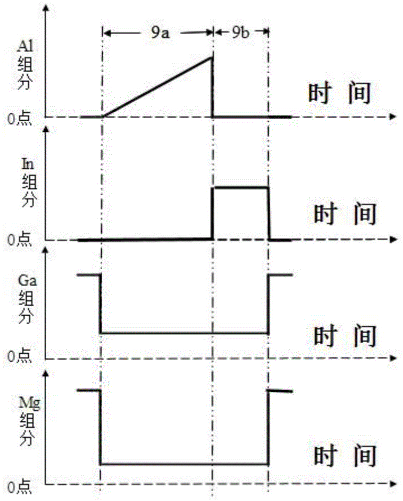
[0026] A P-type insertion layer with a cyclic structure and its growth method, the order of its epitaxial structure from bottom to top is: substrate, low-temperature GaN buffer layer, GaN undoped layer, N-type GaN layer, multi-quantum well structure MQW, The growth method of the low-temperature P-type GaN layer, P-type AlGaN layer, high-temperature P-type GaN layer and P-type contact layer includes the following specific steps:

[0027] (1) Clean the sapphire substrate at a high temperature for 10 minutes in a hydrogen atmosphere at 1050°C, and then perform nitriding treatment;

[0028] (2) Cool down to 500°C, grow a low-temperature GaN buffer layer with a thickness of 25nm, the growth pressure is 500mbar, and the V / III ratio is 200;

[0029] (3) After the growth of the low-temperature GaN buffer layer is completed, stop feeding trimethylgallium (TMGa), raise the substrate temperature to 800°C, and perform in-situ thermal annealing on the low-temperature GaN buffer layer. The ...

Embodiment 2

[0041] A P-type insertion layer with a cyclic structure and its growth method, the order of its epitaxial structure from bottom to top is: substrate, low-temperature GaN buffer layer, GaN undoped layer, N-type GaN layer, multi-quantum well structure MQW, The growth method of the low-temperature P-type GaN layer, P-type AlGaN layer, high-temperature P-type GaN layer and P-type contact layer includes the following specific steps:

[0042] (1) Clean the sapphire substrate at a high temperature for 15 minutes in a hydrogen atmosphere at 1150°C, and then perform nitriding treatment;

[0043] (2) Cool down to 600°C, grow a low-temperature GaN buffer layer with a thickness of 40nm, the growth pressure is 800mbar, and the V / III ratio is 800;

[0044] (3) After the growth of the low-temperature GaN buffer layer is completed, stop feeding trimethylgallium (TMGa), raise the substrate temperature to 1050°C, and perform in-situ thermal annealing on the low-temperature GaN buffer layer. The...

Embodiment 3

[0056] A P-type insertion layer with a cyclic structure and its growth method, the order of its epitaxial structure from bottom to top is: substrate, low-temperature GaN buffer layer, GaN undoped layer, N-type GaN layer, multi-quantum well structure MQW, The growth method of the low-temperature P-type GaN layer, P-type AlGaN layer, high-temperature P-type GaN layer and P-type contact layer includes the following specific steps:

[0057] (1) Clean the sapphire substrate at a high temperature for 12 minutes in a hydrogen atmosphere at 1100°C, and then perform nitriding treatment;

[0058] (2) Cool down to 550°C, grow a low-temperature GaN buffer layer with a thickness of 30nm, the growth pressure is 600mbar, and the V / III ratio is 300;

[0059] (3) After the growth of the low-temperature GaN buffer layer is completed, stop feeding trimethylgallium (TMGa), raise the substrate temperature to 900°C, and perform in-situ thermal annealing on the low-temperature GaN buffer layer. The ...


PUM


Abstract

The invention provides a P (Positive) type insert layer with a cycle structure and a growing method. An epitaxial structure of the P type insert layer comprises a substrate, a low-temperature GaN buffer layer, a GaN undoped layer, an N (Negative) type GaN layer, an MQW (Multiple Quantum Well) structure, a low-temperature P type GaN layer, a P type AlGaN layer, a high-temperature P type GaN layer and a P type contact layer in sequence from bottom to top; the growing method of the P type insert layer comprises the following specific steps that a PAlGaN / PinGaN cycle structure layer grows; the structure comprises three to ten structures that PGaN and PInGaN grow in an overlapping way; the growth is divided into two steps, i.e. growing an Al component to gradually raise the PAlGaN layer at first, and after the completion of growth that the PAlGaN layer is gradually raised along with the Al component, growing the PInGaN layer, and then continuously growing six PAlGaN layer / PInGaN layer cycles. According to the P type insert layer and the growing method, the dislocation density of PGaN can be decreased, and the crystalline quality can be improved; in addition, the generation of non-radiating load centers is inhibited, and the injection efficiency of cavities is improved, so that the light emitting efficiency of a gallium-nitride-based LED (Light Emitting Diode) is improved; thirdly, the diffusion of Mg atoms towards an active area is reduced, so that the internal quantum efficiency is improved.

Description

technical field [0001] The invention relates to the technical field of preparation of Group III nitride materials, in particular to a P-type insertion layer with a cyclic structure and a growth method. Background technique [0002] Light Emitting Diode (LED, Light Emitting Diode) is a semiconductor solid light-emitting device. By applying a forward voltage across the device, electrons and holes recombine in the active region to generate a large number of photons, and the electrical energy is converted into light energy. Gallium nitride-based semiconductors are the third-generation semiconductor materials after Si and GaAs, and have developed rapidly in recent years. Group III nitrides including GaN, InN, AlN and ternary and quaternary solid solutions are all direct bandgap wide bandgap materials, and their bandgap ranges from 0.7eV of InN to 6.28eV of AlN. InGaAlN has become the material with the widest bandgap across the bandgap and has been widely used in blue-green light...

Claims


Application Information

Patent Timeline
Patent Type & Authority Patents(China)
IPC IPC(8): H01L33/32H01L33/00
CPCC30B25/16C30B29/403C30B29/406H01L33/007
Inventor 肖云飞
Owner 宁波安芯美半导体有限公司
Why Eureka
Try Eureka