
Eureka
For R&D, Eureka makes reading and utilizing patents & technical documents easy.
Eureka AIR
Designed for self-driven R&D workflows. Generate viable solutions, solve complex R&D challenges, empower your innovation with AI.

Eureka Materials
Designed for material experts only. Revolutionize your material R&D, from search, analyze, to developing new materials.

TechResearch
Generate reliable direction feasibility study reports for your R&D in just a few steps.

TechSeek
Discover and master advanced knowledge NOW. Basics, ideas, possibilities, all at once.

TechMind
As an expert in R&D Theories, TechMind can generates customized viable solutions instantly.

TechRisk
Analyze your overall solution with one click, know your potential R&D risks in advance.

TechMonitor
Get weekly tech updates, stay abreast of the latest tech innovations and key insights.
Array substrate, preparation method thereof and organic electroluminescence display device
A technology of array substrate and light-emitting layer, applied in circuits, photovoltaic power generation, electrical components, etc., can solve the problem of total reflection light-emitting efficiency at the interface between electrode layer and substrate, and achieve the effect of enhancing light-emitting efficiency
- Summary
- Abstract
- Description
- Claims
- Application Information
AI Technical Summary
Problems solved by technology
Method used
Image

Examples
Embodiment 1
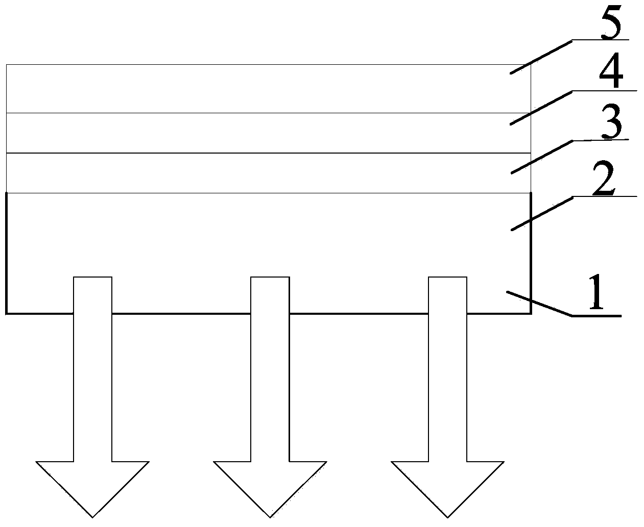
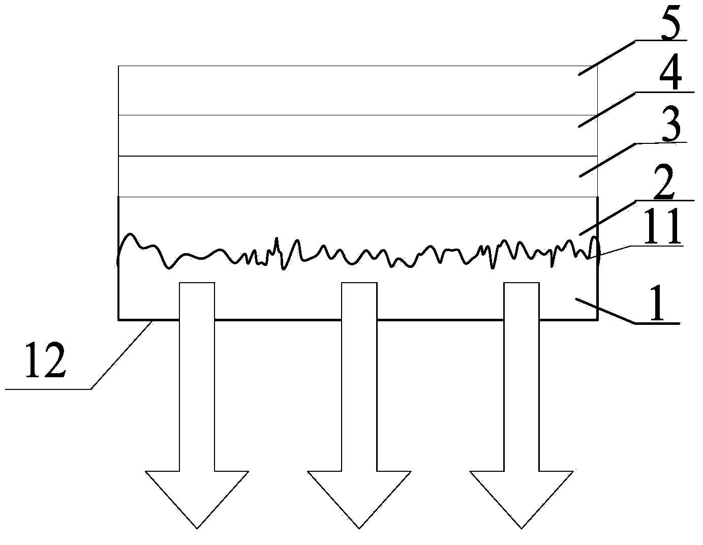
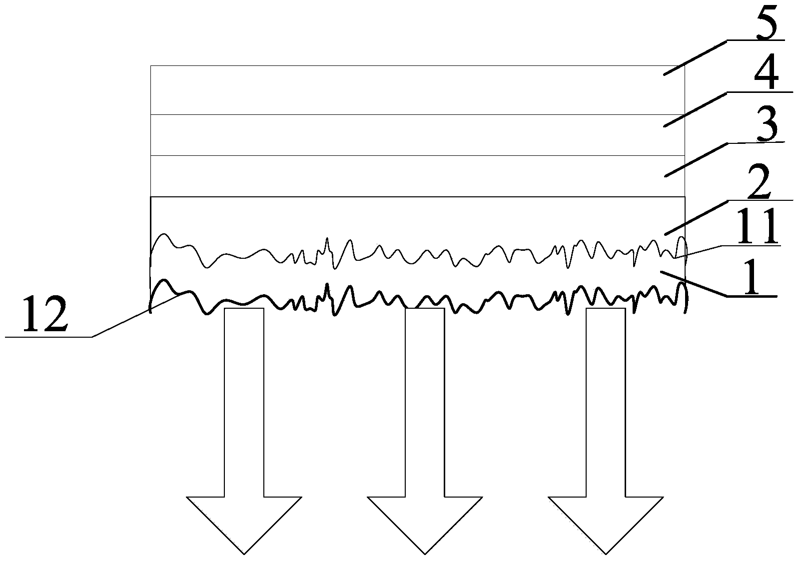
[0031] like figure 2 As shown, this embodiment provides an array substrate, including a substrate 1, a planarization layer 2, a light-emitting layer 4 arranged in sequence on the substrate 1, and electrode layers located on both sides of the light-emitting layer 4 for supplying voltage to the light-emitting layer 4 , the side of the substrate 1 close to the light-emitting layer 4 is the inner surface 11, the inner surface 11 is a rough surface, the electrode layer between the inner surface 11 and the light-emitting layer 4 is the first electrode layer 3, and the other side of the light-emitting layer 4 is the first electrode layer 3. The side is the second electrode layer 5, and the above-mentioned first electrode layer and the second electrode layer can be the cathode electrode layer and the anode electrode layer, respectively.
[0032] Since the inner side surface 11 of the substrate 1 of the array substrate of the present invention is a rough surface, light ( figure 2 In...
Embodiment 2
[0043] This embodiment provides a method for preparing the above-mentioned array substrate, which includes the following steps:
[0044] 1) Prepare a substrate with at least one rough surface;
[0045] The substrate 1 in this embodiment is a glass substrate, and the glass can also be roughened by using the processing methods in the prior art, such as grinding with a grinding wheel or etching with a hydrogen fluoride solution, etc., to control the roughness of the rough surface Ra in the range of 5-500nm , where Ra is the arithmetic mean deviation of the contour. The glass substrate of the present embodiment is polished with a grinding wheel to form a glass substrate with a rough surface, wherein the Ra of the roughness of the glass substrate is 300 nm.
[0046] It should be understood that commercially available glass substrates with rough surfaces can be used as glass substrates with rough surfaces; for substrates prepared from other materials, known methods can be used in t...
Embodiment 3
[0057] This embodiment provides an organic electroluminescent display device, which includes the above-mentioned organic electroluminescent array substrate.
PUM
 Abstract
Description
Claims
Application Information
 - R&D Engineer
- R&D Manager
- IP Professional
- Industry Leading Data Capabilities
- Powerful AI technology
- Patent DNA Extraction
Browse by: Latest US Patents, China's latest patents, Technical Efficacy Thesaurus, Application Domain, Technology Topic, Popular Technical Reports.
© 2024 PatSnap. All rights reserved.Legal|Privacy policy|Modern Slavery Act Transparency Statement|Sitemap|About US| Contact US: help@patsnap.com