
Thin film transistor array substrate, liquid crystal display device and manufacturing method

A technology for thin film transistors and array substrates, which is applied in the field of low temperature polysilicon liquid crystal display, can solve the problems of increasing complexity and manufacturing cost, increasing process difficulty, and deteriorating display effect, so as to improve display performance, reduce process difficulty and cost, The effect of reducing the number of times

Active Publication Date: 2014-06-25
XIAMEN TIANMA MICRO ELECTRONICS
View PDF4 Cites 34 Cited by
  • Summary
  • Abstract
  • Description
  • Claims
  • Application Information

AI Technical Summary

Problems solved by technology

More masking processes will significantly increase the complexity and cost of manufacturing. At the same time, the difference in mutual coverage between the layers of the existing array substrate structure will lead to poor display effects and increase the difficulty of the process.

Method used


Image

  • Thin film transistor array substrate, liquid crystal display device and manufacturing method
  • Thin film transistor array substrate, liquid crystal display device and manufacturing method
  • Thin film transistor array substrate, liquid crystal display device and manufacturing method

Examples


Embodiment Construction

[0063] The technical solutions of the present invention will be further described below in conjunction with the accompanying drawings and through specific implementation methods.

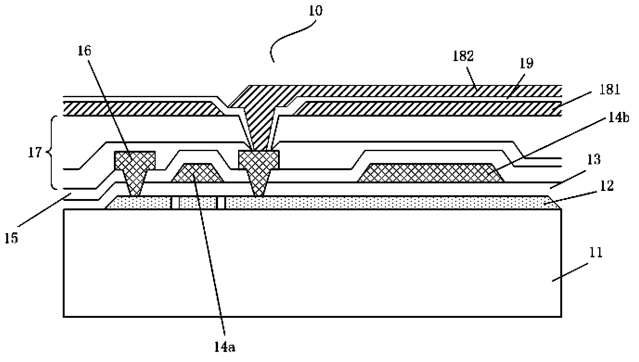
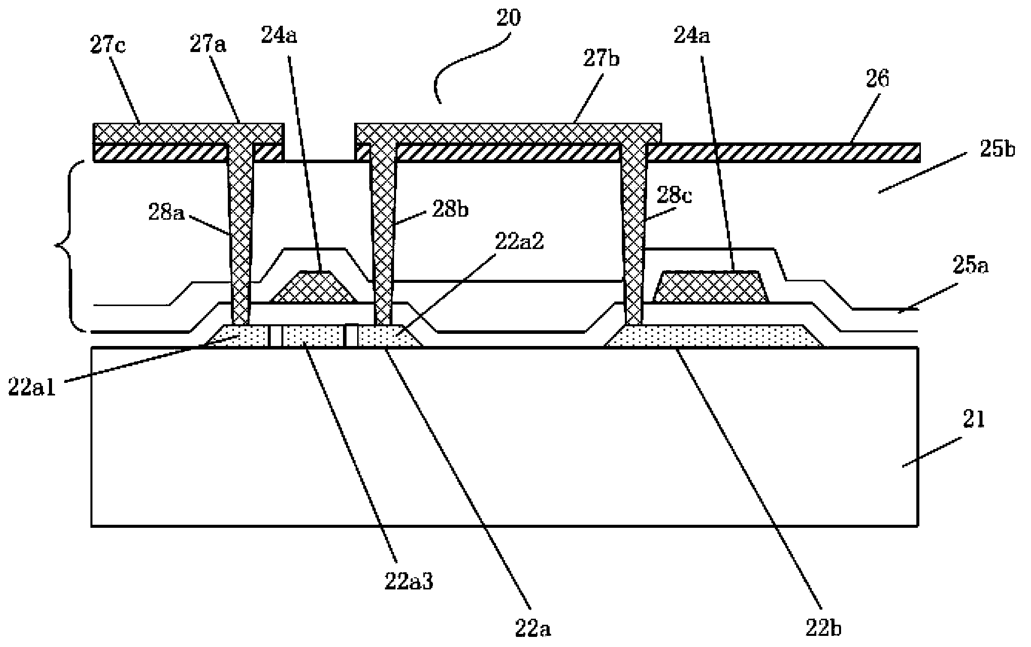
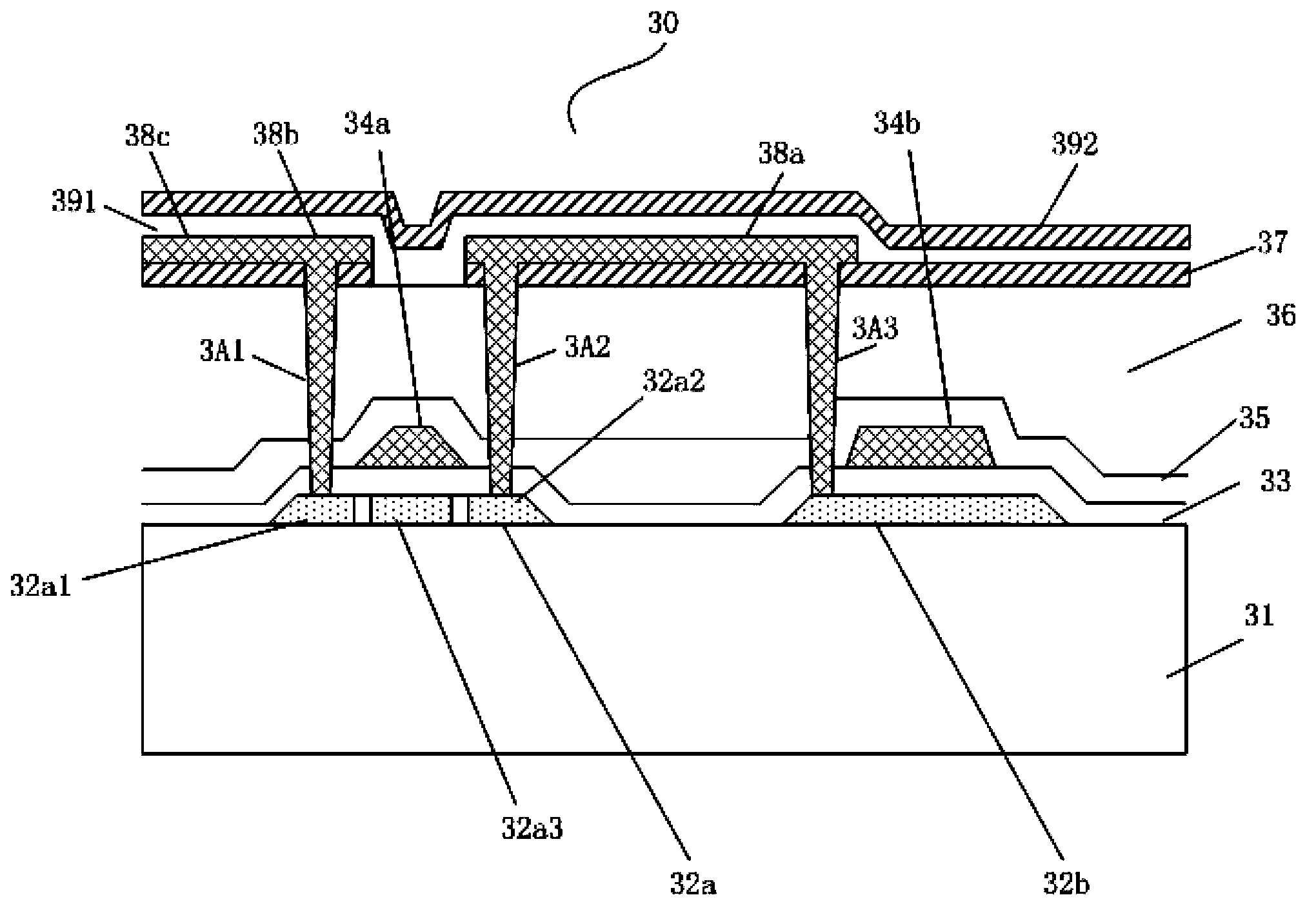
[0064] figure 2 is a schematic cross-sectional view of the low temperature polysilicon thin film transistor array substrate according to the first embodiment of the present invention. Such as figure 2 As shown, the array substrate 20 includes a substrate 21; a patterned active layer 22; a gate insulating layer 23 covering the active layer; a patterned first metal layer 24 disposed on the gate insulating layer; The protection layer 25 of the first metal layer; the patterned first transparent conductive layer 26 disposed on the protection layer 25 and the patterned second metal layer 27 disposed on the first transparent conductive layer 26 .

[0065] Wherein, the first metal layer 24 includes a gate 24a and a gate line 24b, and the gate line 24b is used as a scan line of the array substrate to sel...


PUM


Abstract

The invention discloses a low-temperature poly-silicon thin film transistor array substrate, a liquid crystal display device and a corresponding manufacturing method. The thin film transistor array substrate is used for forming the source electrode of the thin film transistor and the drain electrode of the thin film transistor, and the mental layer of an array substrate data line is formed on a transparent conductive layer of a pixel electrode, such that only one-time via hole patterning technology needs to be carried out during the manufacturing process. As the metal layer and the transparent conductive layer are stacked together, two layers of patterning can be realized by using half transparent mask technology for one-time etching, times of the mask exposure technology are reduced, and the technology difficulty and the cost can be reduced.

Description

technical field [0001] The invention relates to the field of low-temperature polysilicon liquid crystal display, in particular to a low-temperature polysilicon thin film transistor array substrate, a liquid crystal display device and a manufacturing method thereof. Background technique [0002] The low temperature polysilicon thin film transistor (LTPS-TFT, Low Temperature Poly-Silicon Thin Film Transistor) array substrate used in the existing low temperature polysilicon liquid crystal display device usually uses such as figure 1 structure shown. Such as figure 1 As shown, the thin film transistor array substrate 10 includes a substrate 11, an active layer 12, a gate insulating layer 13, a patterned first metal layer 14 including a gate pattern 14a and a gate line pattern 14b, a first protective layer 15, and a The second metal layer 16 patterned on the first protective layer 15, the second protective layer 17 and the transparent conductive layer 181 on the second protecti...

Claims


Application Information

Patent Timeline
IPC IPC(8): H01L29/417H01L23/50H01L27/12H01L21/28H01L21/84
CPCH01L27/124H01L21/28017H01L23/5283H01L23/5286H01L27/1288
Inventor 谢振清李俊谊周晓莲
Owner XIAMEN TIANMA MICRO ELECTRONICS
Features
  • Generate Ideas
  • Intellectual Property
  • Life Sciences
  • Materials
  • Tech Scout
  • Unparalleled Data Quality
  • Higher Quality Content
  • 60% Fewer Hallucinations
Learn More