Floating gate preparation method

A floating gate and wet etching technology, which is applied to semiconductor devices, electrical components, circuits, etc., can solve the problem of low coupling rate of floating gate and control gate, and achieve the effect of avoiding short circuit

Active Publication Date: 2014-07-02
GIGADEVICE SEMICON (BEIJING) INC
View PDF8 Cites 8 Cited by
  • Summary
  • Abstract
  • Description
  • Claims
  • Application Information

AI Technical Summary

Problems solved by technology

[0005] The present invention aims to provide a method for preparing a floating gate to solve the risk of a short circuit between the active region and the control gate or between the floating gate and the subsequent formation of the existing technology in the process of removing part of the silicon oxide layer in the trench region. Technical problem with small coupling ratio between control gates

Method used


Image

  • Floating gate preparation method
  • Floating gate preparation method
  • Floating gate preparation method

Examples


Embodiment Construction

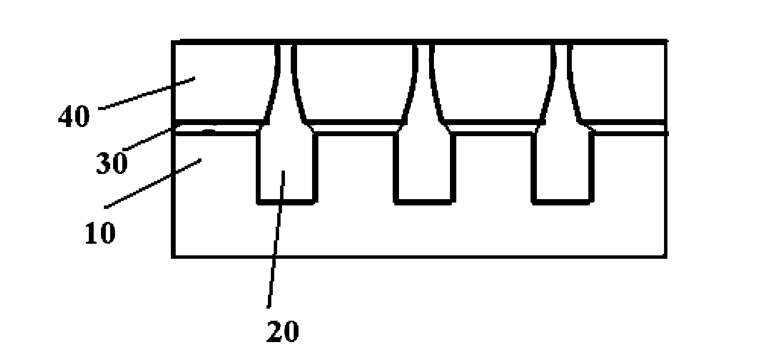
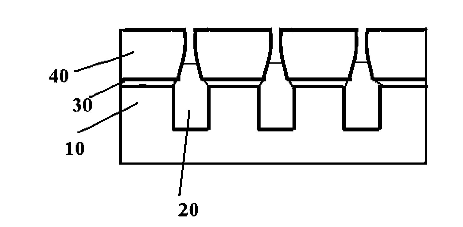
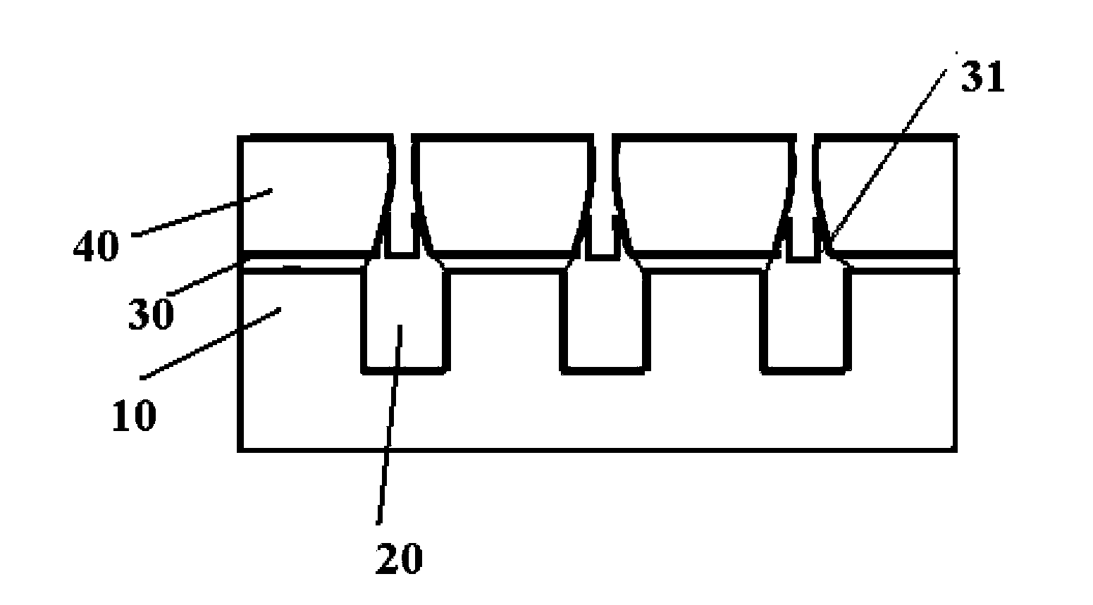
[0021] It should be noted that, in the case of no conflict, the embodiments in the present application and the features in the embodiments can be combined with each other. The present invention will be described in detail below with reference to the accompanying drawings and examples.

[0022] For the convenience of description, spatially relative terms, such as "on", "over", "above", etc., may be used here to describe The spatial positional relationship between one device or feature shown and other devices or features. It will be understood that the spatially relative terms are intended to encompass different orientations of the device in use or operation in addition to the orientation depicted in the figures. For example, if the device in the figures is turned over, devices described as "above" or "above" other devices or configurations would then be oriented "beneath" or "above" the other devices or configurations. under other devices or configurations". Thus, the exempl...


PUM


Abstract

The invention discloses a floating gate preparation method. The method comprises steps: S1, a shallow trench isolation structure whose upper surface is higher than the first height H1 of the upper surface of a semiconductor substrate is formed on a semiconductor substrate; S2, an active region is formed on the semiconductor substrate through ion implantation; S3, a tunnel oxide layer is formed on the semiconductor substrate; S4, a floating gate material layer is deposited on the tunnel oxide layer; S5, the floating gate material layer is flattened to enable the upper surface of the shallow trench isolation structure to be exposed; and S6, part of the shallow trench isolation structure is removed by etching to form the floating gate. S6 further comprises steps of adopting wet etching to remove the shallow trench isolation structure with a second height H2 to enable coupling efficiency between the floating gates and control gates formed subsequently to be high, and adopting dry etching to remove the shallow trench isolation structure with a third height H3 to form the floating gates. When the technical scheme of the invention is applied, the coupling efficiency between the floating gate and control gates formed subsequently is high, and the risk of short circuit between the active region and the control gates can be avoided.

Description

technical field [0001] The invention relates to the technical field of integrated circuit device manufacturing, in particular to a method for preparing a floating gate. Background technique [0002] In recent years, the application of high-density flash memory in many fields has received great attention, because the reduction of the size of the storage unit can greatly reduce the manufacturing cost. [0003] Currently, there are many methods for forming floating gates of integrated circuit devices. Among them, a typical floating gate preparation method is as follows: 1) Provide a semiconductor substrate, such as a silicon wafer, silicon insulator or epitaxial silicon wafer; 2) use a high-density plasma process to deposit a pad silicon oxide layer and a silicon nitride layer, Etching to form a trench region; filling the trench region and above the surface of the silicon nitride layer; 3) using a chemical mechanical polishing process to planarize the silicon oxide layer depos...

Claims


Application Information

Patent Timeline
Patent Type & Authority Applications(China)
IPC IPC(8): H01L21/28
CPCH01L29/40114H10B41/00
Inventor 贾硕冯骏魏征
Owner GIGADEVICE SEMICON (BEIJING) INC
Why Eureka
Try Eureka