Method for stripping and transferring gallium arsenide based epitaxial layer

A gallium arsenide-based, lift-off transfer technology, applied in the field of semiconductor technology, to achieve the effect of not easy to wrinkle or break, good uniformity, and not easy to fragment

Inactive Publication Date: 2014-07-02
NO 55 INST CHINA ELECTRONIC SCI & TECHNOLOGYGROUP CO LTD
View PDF6 Cites 11 Cited by
  • Summary
  • Abstract
  • Description
  • Claims
  • Application Information

AI Technical Summary

Problems solved by technology

[0005] The present invention proposes a method for peeling off and transferring gallium arsenide-based epitaxial layers, and its purpose is to solve the problem of heterogeneous integration between gallium arsenide-based epitaxial layers and different semiconductor materials

Method used


Image

  • Method for stripping and transferring gallium arsenide based epitaxial layer
  • Method for stripping and transferring gallium arsenide based epitaxial layer
  • Method for stripping and transferring gallium arsenide based epitaxial layer

Examples


Embodiment 1

[0038] ① Soak the gallium arsenide-based epitaxial wafer and glass slide in diluted hydrochloric acid (HCl) for 60 seconds, then rinse with deionized water, and put them in a spin dryer for drying.

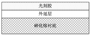
[0039] ② Spin-coat the positive photoresist on the front surface of the GaAs-based epitaxial wafer, the rotation speed is 5000 rpm, and the spin-coating time is 90 seconds.

[0040] ③ Put the GaAs-based epitaxial wafer coated with positive photoresist facing up on the heating plate, the temperature of the hot plate is 110 degrees Celsius, and the baking time is 5 minutes.

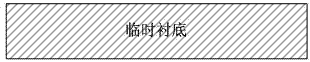
[0041] ④Take the gallium arsenide-based epitaxial wafer from the hot plate and stack it with the front of the glass slide, fix it with a fixture and put it into a bonding machine for bonding. The bonding temperature is 200 degrees Celsius and the bonding time is 60 minutes.

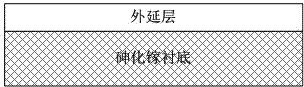
[0042] ⑤ After bonding, thin the back of the gallium arsenide substrate of the gallium arsenide-based epitaxial wafer to about 100 micron...

Embodiment 2

[0048] ① Soak the gallium arsenide-based epitaxial wafer and glass slide in diluted hydrochloric acid (HCl) for 30 seconds, then rinse with deionized water, and put them in a spin dryer for drying.

[0049]② Spin-coat positive photoresist on the front surface of the GaAs-based epitaxial wafer, the rotation speed is 1000 rpm, and the spin-coating time is 60 seconds.

[0050] ③ Put the GaAs-based epitaxial wafer coated with positive photoresist facing up on the heating plate, the temperature of the hot plate is 100 degrees Celsius, and the baking time is 2 minutes.

[0051] ④Take the gallium arsenide-based epitaxial wafer from the hot plate and stack it with the front of the glass slide, fix it with a fixture and put it into a bonding machine for bonding. The bonding temperature is 180 degrees Celsius and the bonding time is 30 minutes.

[0052] ⑤ After bonding, thin the back of the gallium arsenide substrate of the gallium arsenide-based epitaxial wafer to about 100 microns, an...


PUM


Abstract

The invention discloses a method for stripping and transferring a gallium arsenide based epitaxial layer. The method comprises the steps of (1) cleaning surfaces of a gallium arsenide based epitaxial piece and a temporary substrate through dilute hydrochloric acid; (2) spin-coating photoresist on the front surface of the gallium arsenide based epitaxial piece; (3) putting the gallium arsenide based epitaxial piece on a hot plate with the front surface upward to perform baking; (4) bonding the cooled front surface of the gallium arsenide based epitaxial piece with the front surface of the temporary substrate oppositely; (5) removing a gallium arsenide substrate of the gallium arsenide based epitaxial piece; (6) cleaning an objective substrate and the surface of an epitaxial piece supported by the temporary substrate through the dilute hydrochloric acid; (7) spin-coating BCB on the front surface of the epitaxial piece supported by the temporary substrate; (8) putting the epitaxial piece supported by the temporary substrate on the hot plate with the front surface upward to perform baking; (9) bonding the cooled front surface of the epitaxial piece supported by the temporary substrate with the front surface of the objective substrate oppositely; (10) immersing the bonded wafer in acetone, and automatically separating the objective substrate from the temporary substrate after the photoresist is dissolved. The method has the advantages that the epitaxial layer on the gallium arsenide based epitaxial piece can be transferred onto any objective substrate integrally, the process is simple, and the gallium arsenide based epitaxial layer cannot be damaged during transfer.

Description

technical field [0001] The invention relates to a method for stripping and transferring a gallium arsenide-based epitaxial layer, which belongs to the technical field of semiconductor technology. Background technique [0002] With the rapid development of semiconductor process technology, it is also limited by the heterogeneous growth of semiconductor materials to a certain extent. Among them, the integration of different semiconductor materials on the same wafer by using heterogeneous integration technology has become a current research hotspot. [0003] Heteroepitaxial growth is a commonly used method for heterogeneous integration. However, due to the large lattice mismatch between semiconductor materials, the semiconductor material grown by heteroepitaxial growth contains a high dislocation density, which changes the material properties. The device is thus unusable. For heterogeneous materials with large mismatch, the heteroepitaxial growth technology has certain difficu...

Claims


Application Information

Patent Timeline
Patent Type & Authority Applications(China)
IPC IPC(8): H01L21/683
CPCH01L21/6835H01L2221/68386
Inventor 吴立枢赵岩程伟
Owner NO 55 INST CHINA ELECTRONIC SCI & TECHNOLOGYGROUP CO LTD
Why Eureka
Try Eureka