Antenna device and method for making antenna

An antenna device and high dielectric layer technology, applied in the field of electronics, can solve the problems of large space, large volume of FPC antenna, large antenna space, etc., and achieve the effect of reducing space

Active Publication Date: 2018-10-12
LENOVO (BEIJING) LTD
View PDF5 Cites 0 Cited by
  • Summary
  • Abstract
  • Description
  • Claims
  • Application Information

AI Technical Summary

Problems solved by technology

The traditional FPC antenna has a large volume, which requires a large space to place it, and it is difficult to reduce the space it occupies
Traditional chip antennas are usually placed on the main printed circuit board of electronic equipment. Although the chip antenna is small in size, it requires a good space environment, such as a large design clearance, so the actual antenna space required by the chip antenna is relatively large

Method used


Image

  • Antenna device and method for making antenna
  • Antenna device and method for making antenna
  • Antenna device and method for making antenna

Examples


Embodiment Construction

[0031] The following will clearly and completely describe the technical solutions in the embodiments of the present invention with reference to the accompanying drawings in the embodiments of the present invention. Obviously, the described embodiments are some of the embodiments of the present invention, but not all of them.

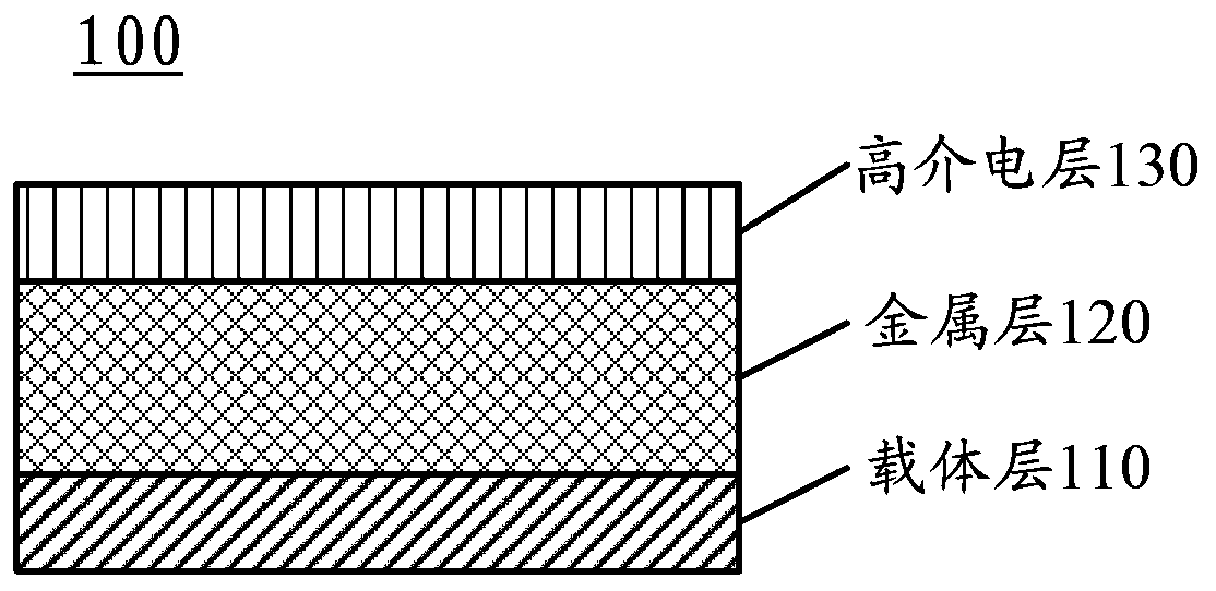
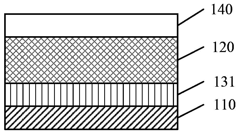
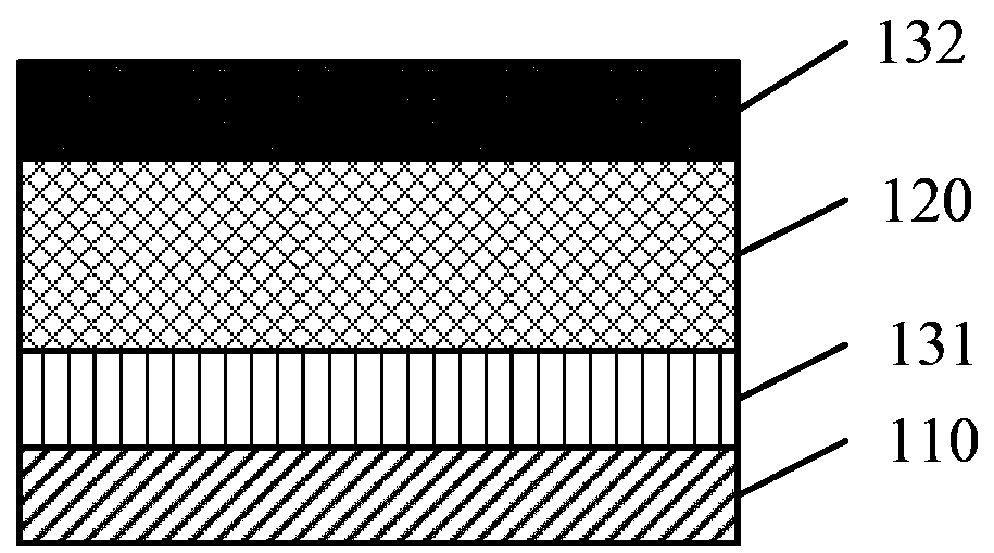
[0032] In the present invention, when it is described that a specific layer is located on another layer, there may or may not be an intervening layer between the specific layer and the other layer; when it is described that a specific layer is located on the first layer and the second layer, there may or may not be an intervening layer between the specific layer and the first layer or the second layer; when it is described that a specific layer directly contacts another layer, in the There are no intervening layers between a particular layer and that other layer.

[0033] FPC is a printed circuit made of flexible insulating substrate, which has many adva...


PUM


Abstract

The invention provides an antenna device and an antenna fabrication method. The antenna device comprises: a carrier layer which is the base carrier of the antenna device; a metal layer which is located on the carrier layer and used as an radiating body to transmitting and receiving signals; and a high-dielectric layer which is in contact with the metal layer directly and mode from a high-dielectric material of which the dielectric constant is greater than a preset threshold. In the technical scheme of the antenna device and the antenna fabrication method according to the embodiments of the invention, by arranging the high-dielectric layer which is in contact with the metal layer directly, the occupied space of the antenna can be reduced.

Description

technical field [0001] The present invention relates to the field of electronic technology, and more particularly, to an antenna device and a method for manufacturing the antenna. Background technique [0002] With the development of communication technology, various types of electronic equipment, such as computers, personal digital assistants, mobile communication terminals, etc., appear. The electronic device has the function of wireless communication, thereby greatly facilitating the transmission of information and data. As a consumer electronic product, the electronic device is developing toward miniaturization, for example, its thickness is getting thinner and its volume is getting smaller and smaller. As the thickness and volume of electronic devices become thinner, the space occupied by antennas, as an important part of wireless communication devices, is correspondingly compressed, which increases the difficulty of antenna design. [0003] Existing antennas include,...

Claims


Application Information

Patent Timeline
Patent Type & Authority Patents(China)
IPC IPC(8): H01Q1/38H01Q1/40
Inventor 万波刘瑾
Owner LENOVO (BEIJING) LTD
Why Eureka
Try Eureka