Liquid crystal panel and thin-film transistor substrate

A technology of liquid crystal display panels and thin film transistors, which is applied in nonlinear optics, instruments, optics, etc., can solve problems such as alignment deviation, liquid crystal display panel aperture ratio or display effect reduction, etc., so as to improve aperture ratio and facilitate alignment Position, improve the effect of alignment deviation

Inactive Publication Date: 2014-07-09
HONG FU JIN PRECISION IND (SHENZHEN) CO LTD +1
View PDF10 Cites 18 Cited by
  • Summary
  • Abstract
  • Description
  • Claims
  • Application Information

AI Technical Summary

Problems solved by technology

However, since the thin film transistor substrate and the color filter substrate are manufactured independently and then bonded together through the frame glue, when the thin film transistor substrate and the color filter substrate are combined, the color filter layer, the thin film transistor and the driver Alignment deviation is prone to occur between lines, which may lead to a decrease in the aperture ratio or display effect of the LCD panel

Method used


Image

  • Liquid crystal panel and thin-film transistor substrate
  • Liquid crystal panel and thin-film transistor substrate

Examples


Embodiment Construction

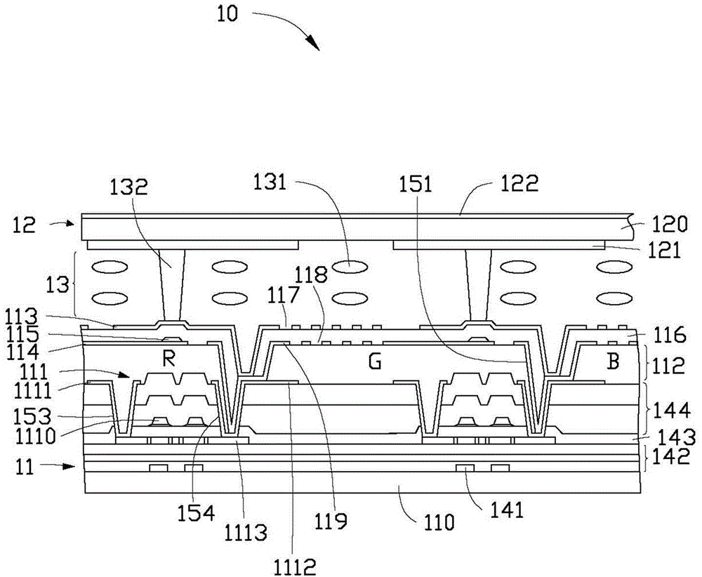
[0042] see figure 1 , figure 1 It is a schematic cross-sectional view of the first embodiment of the liquid crystal display panel 10 of the present invention (wherein the cross-section may include a stepped cross-section). The liquid crystal display panel 10 includes a first substrate 11, a second substrate 12 opposite to the first substrate 11, and a liquid crystal layer 13 interposed between the first substrate 11 and the second substrate 12. The first substrate 11 Including a first substrate 110, a thin film transistor 111 disposed on the first substrate 110, a passivation layer 112 covering the thin film transistor 111, a pixel electrode 113 electrically connected to the thin film transistor 111, and a pixel electrode 113 insulated from the pixel electrode 113 common electrode layer 114 . In this embodiment, the passivation layer 112 is also used as a color filter layer, and the color filter layer is a part of the color filter of the liquid crystal display panel 10 . In...


PUM


Abstract

The invention provides a liquid crystal panel and a thin-film transistor substrate. The liquid crystal display panel comprises a first substrate, a second substrate and a liquid crystal layer, wherein the first substrate comprises a first base, thin-film transistors arranged on the first substrate, a passivation layer covering the thin-film transistors, a pixel electrode electrically connected with the thin-film transistors and a common electrode layer insulated from the pixel electrode. The common electrode layer and the pixel electrode generate liquid crystal molecules parallel to an electric field driving liquid crystal layer to rotate in a plane, and the passivation layer comprises a color filtering layer. The liquid crystal display panel is high in aperture ratio.

Description

technical field [0001] The invention relates to a liquid crystal display panel and a thin film transistor substrate. Background technique [0002] A liquid crystal display panel generally includes a thin film transistor substrate, a color filter substrate disposed opposite to the thin film transistor substrate, and a liquid crystal layer sandwiched between the two substrates. Generally, a transparent conductive layer (such as a pixel electrode layer) and an opaque thin film transistor and driving circuit are arranged on the thin film transistor substrate, and a color filter layer and a black matrix are arranged on the color filter substrate, wherein the color filter The optical layer needs to be set corresponding to the transparent conductive layer, and the black matrix needs to be set corresponding to the thin film transistor and the driving circuit. However, since the thin film transistor substrate and the color filter substrate are manufactured independently and then bon...

Claims


Application Information

Patent Timeline
Patent Type & Authority Applications(China)
IPC IPC(8): G02F1/1335G02F1/1343
Inventor 廖金阅
Owner HONG FU JIN PRECISION IND (SHENZHEN) CO LTD
Why Eureka
Try Eureka