Light emitting diode packaging structure and manufacturing method thereof

A technology of light-emitting diodes and packaging structures, applied in electrical components, electrical solid-state devices, circuits, etc., can solve problems such as poor alignment of light-emitting diodes, and achieve the effects of improving poor alignment and improving yield.

Active Publication Date: 2020-03-24
UNIMICRON TECH CORP
View PDF9 Cites 2 Cited by
  • Summary
  • Abstract
  • Description
  • Claims
  • Application Information

AI Technical Summary

Problems solved by technology

[0003] The invention provides a packaging structure of light emitting diodes, which can improve the problem of poor alignment of light emitting diodes during transfer, and improve the transfer yield

Method used


Image

  • Light emitting diode packaging structure and manufacturing method thereof
  • Light emitting diode packaging structure and manufacturing method thereof
  • Light emitting diode packaging structure and manufacturing method thereof

Examples


Embodiment Construction

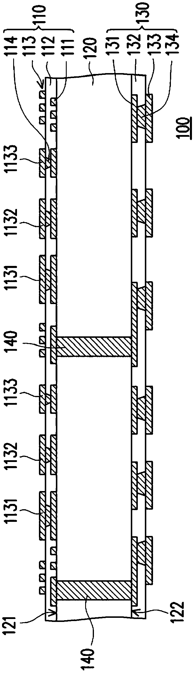
[0029] Figure 1A to Figure 1E It is a schematic cross-sectional view showing a manufacturing method of a light-emitting diode packaging structure according to an embodiment of the present invention.

[0030] Please refer to Figure 1A , forming a carrier 100 , and the carrier 100 at least includes a first build-up circuit 110 . In detail, in this embodiment, the substrate 120 is firstly provided, and the substrate 120 is drilled, for example by laser, to form openings penetrating the substrate 120 . Next, a conductive material is filled into the hole to form a conductive via hole 140 , a first build-up circuit 110 is formed on the upper surface 121 of the substrate 120 , and a second build-up circuit 130 is formed on the lower surface 122 of the substrate 120 . Wherein, the first build-up circuit 110 includes a first conductive layer 111 , a first dielectric layer 112 , a second conductive layer 113 and a first conductive hole 114 penetrating through the first dielectric lay...


PUM

PropertyMeasurementUnit
sizeaaaaaaaaaa
sizeaaaaaaaaaa

Abstract

The invention provides a light emitting diode packaging structure and a manufacturing method thereof. The light emitting diode packaging structure comprises a carrier plate, at least one self-assemblymaterial layer, a first solder mask layer and at least one light emitting diode. The carrier plate includes a first build-up line. The self-assembly material layer is disposed on the first build-up circuit. The first solder mask layer is disposed on the first build-up line. The first solder mask layer has at least one opening to expose a portion of the self-assembly material layer. The light emitting diode is disposed on the first build-up circuitry. The light emitting diode has a self-assembled pattern. The light emitting diode is self-assembled in the opening of the first solder mask layerthrough the acting force between the self-assembly pattern and the self-assembly material layer.

Description

technical field [0001] The invention relates to a packaging structure and a manufacturing method thereof, in particular to a self-assembled light emitting diode packaging structure and a manufacturing method thereof. Background technique [0002] Currently, non-solder mask defined (Non-Solder Mask Define, NSMD) structures are mostly used for backplane structures of submillimeter light-emitting diodes (mini LEDs) or micro-light-emitting diodes (Micro LEDs, μLEDs). In order to improve the fineness and resolution of the picture, it needs to be assembled in a high-density matrix arrangement, and a huge amount of transfer work is required. Although the assembly process can use the alignment system of the machine to perform alignment, pick and place parts, thermocompression bonding and other processes to combine the LED die and the backplane, but because the die size is small and the transfer amount is very large, so , if the process of combining with each other only depends on t...

Claims


Application Information

Patent Timeline
Patent Type & Authority Applications(China)
IPC IPC(8): H01L33/62H01L33/38H01L27/15
CPCH01L27/156H01L33/387H01L33/62H01L2933/0016H01L2933/0066
Inventor 林纬廸简俊贤陈富扬
Owner UNIMICRON TECH CORP
Why Eureka
Try Eureka