Semiconductor device including bit line formed using damascene technique and method of fabricating the same

a damascene and semiconductor technology, applied in the field of semiconductor devices, can solve the problems of inability to obtain inability to secure a sufficient process margin, and inability to achieve finer bit line patterns by foregoing conventional methods using photolithographic exposure equipment, etc., and achieve the effect of easy formation

Inactive Publication Date: 2006-12-21
SAMSUNG ELECTRONICS CO LTD
View PDF7 Cites 2 Cited by
  • Summary
  • Abstract
  • Description
  • Claims
  • Application Information

AI Technical Summary

Benefits of technology

[0009] An aspect of the present invention is to provide a method of fabricating a semiconductor device, in which, despite the reduced design rule, bit line patterns can be easily formed and the process margin can be sufficiently secured.
[0010] Another aspect of the present invention is to provide a semiconductor device including a bit line, in which the misalignment margin between the bit line and a storage node contact hole is increased.
[0015] According to various exemplary embodiments of the present invention, formation of a bit line employs not a photolithographic process but a damascene technique. Thus, even a bit line having the reduced design rule can be easily formed. Also, misalignment between a bit line and a lower conductive element (e.g., a bit line contact plug), which occurs due to the reduced design rule, can be minimized. Further, because the dimension of a bit line opening is adjusted by controlling the width of the spacers, a bit line conductive layer can be formed to below the photolithographic limit. In addition, as it is not required to fill a gap between bit lines with a gap fill insulating layer, a void does not occur in the gap fill insulating layer. The present invention is not limited to bit lines but can also be applied to adjacently formed conductive layers, such as, for example, various interconnections or gate lines.

Problems solved by technology

However, as the design rule and chip size of DRAMs decrease, overcoming restrictions of photolithographic processes used to form the DRAMs and securing a sufficient process margin become more complicated.
However, the foregoing conventional method using photolithographic exposure equipment cannot obtain finer bit line patterns.
Thus, sufficiently reducing the cell size becomes difficult.
Also, the misalignment margin between a bit line and a bit line contact plug may be reduced, thus causing problems such as leakage.

Method used


Image

  • Semiconductor device including bit line formed using damascene technique and method of fabricating the same
  • Semiconductor device including bit line formed using damascene technique and method of fabricating the same
  • Semiconductor device including bit line formed using damascene technique and method of fabricating the same

Examples


first embodiment

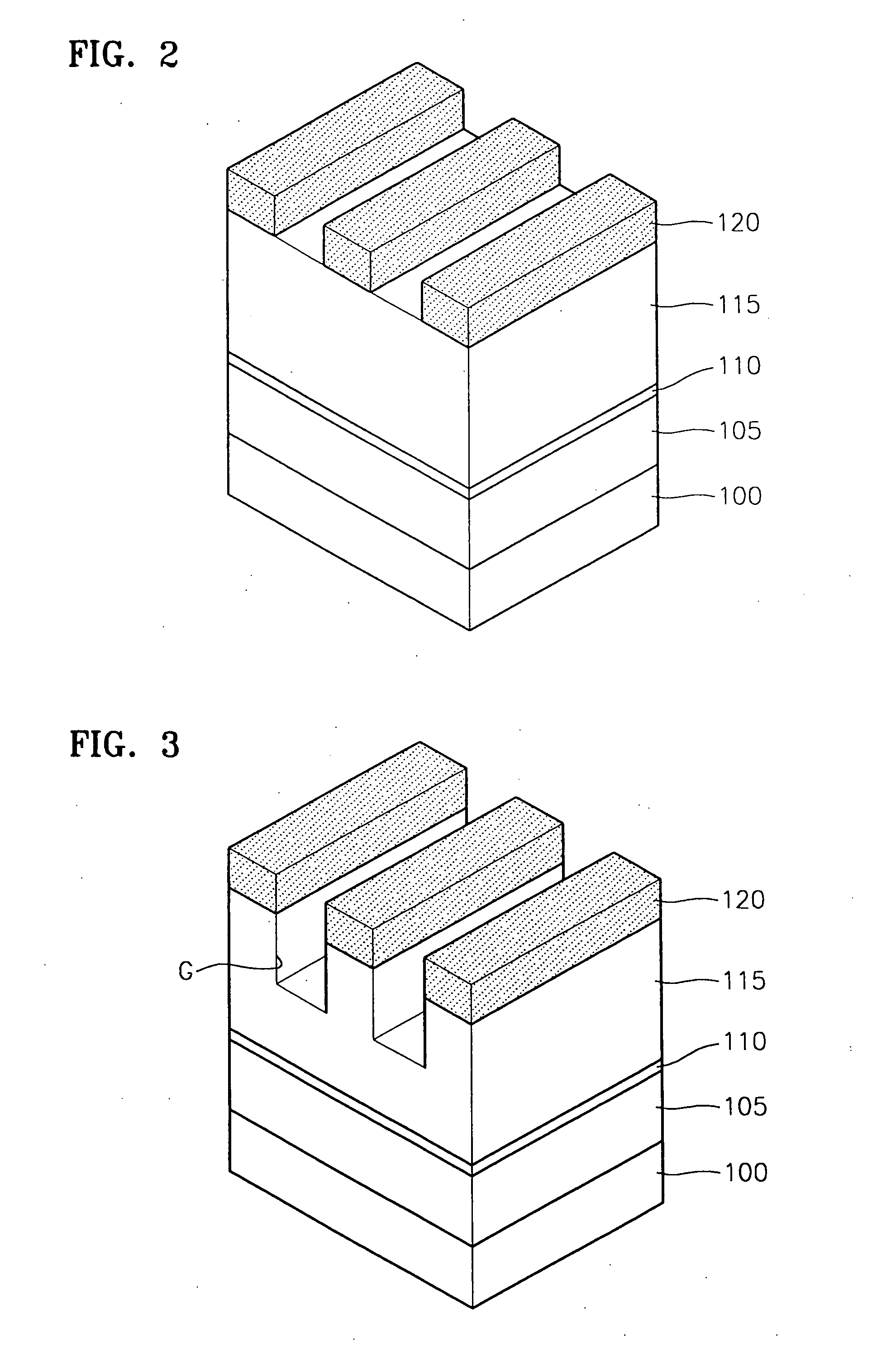
[0022]FIGS. 2 through 9 are cross-sectional views illustrating a method of fabricating a semiconductor device according to the present invention. While the following embodiments will be described with reference to a method of fabricating bit lines of DRAMs, it should be apparent to those skilled in the art that a similar description can be applied to other conductive lines, gate lines, or interconnections.

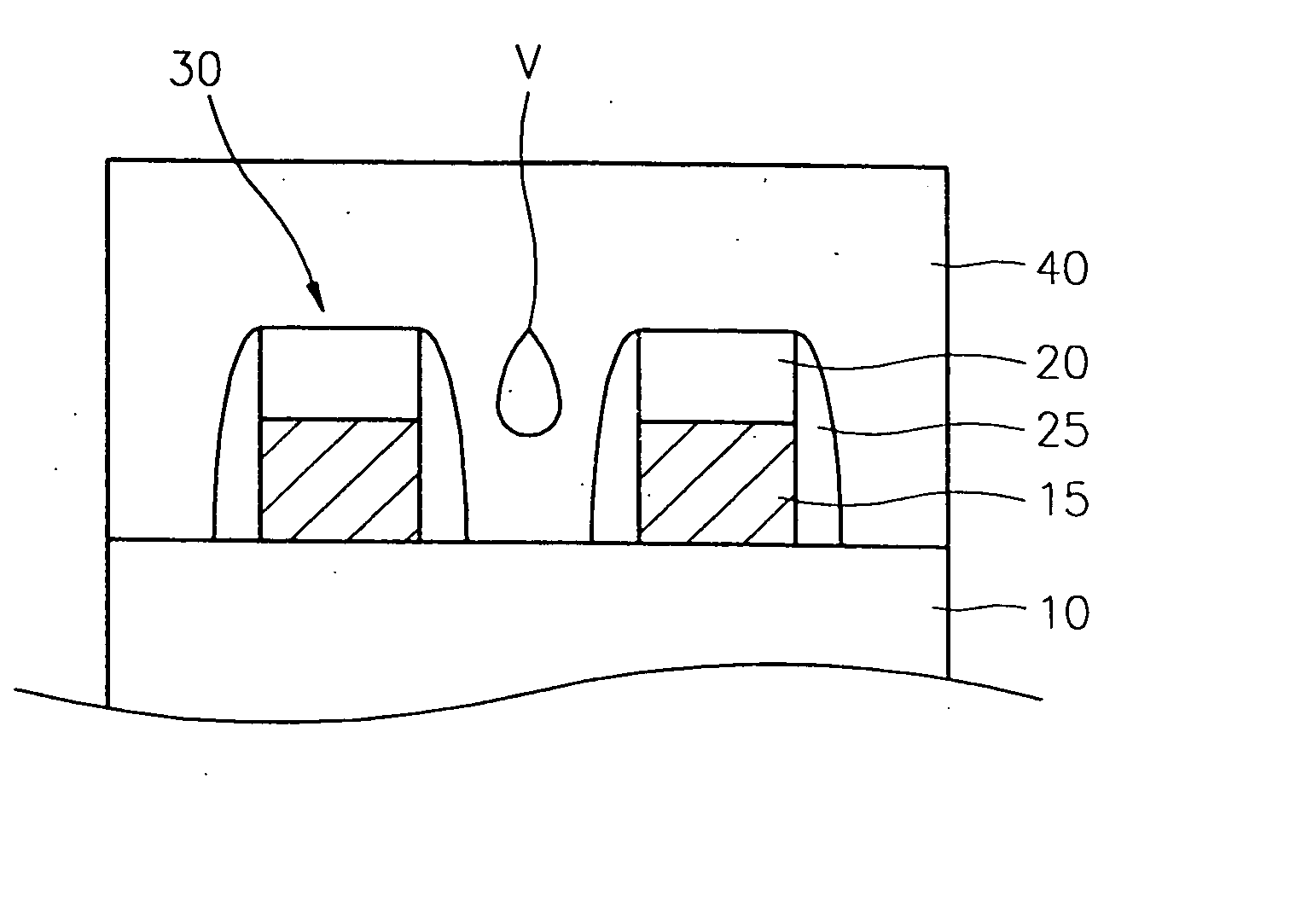
[0023] Referring to FIG. 2, an etch stop layer 110 and a silicon oxide layer 115 are sequentially formed on a substrate 100 on which a lower structure including an insulating layer 105 is formed. The substrate 100 can be, for example, a single crystalline silicon substrate. The etch stop layer 110 is formed of an insulating material having an etch selectivity with respect to the silicon oxide layer 115. For example, the etch stop layer 110 is formed by depositing a silicon nitride layer to a thin thickness using plasma enhanced-CVD (PE-CVD) or low pressure-CVD (LP-CVD). Also, the e...

second embodiment

[0031] Before the second embodiment is described in detail, characteristics of the present embodiment will be described for clarity. In a DRAM, after a bit line contact plug is formed, a silicon nitride layer, which has an etch selectivity with respect to an interlayer dielectric (ILD) (hereinafter, referred to as a “second insulating layer”), is deposited to a thin thickness. The silicon nitride layer is used as an etch stop layer during the formation of a bit line opening to prevent over-etching of a bit line contact plug of a cell array region. Spacers are formed using, for example, silicon nitride, on the inner walls of the bit line opening. As a result, a bit line can be formed to below the photolithographic limit and the misalignment margin between the bit line and a storage node contact plug can be increased.

[0032] Referring to FIG. 10, a device isolation layer 190 (e.g., a shallow trench isolation (STI) layer) is formed on a substrate 200 to define an active region. While th...


PUM


Abstract

A semiconductor device includes an insulating layer having a T-shaped groove formed by a wide opening overlapping a narrow opening, a bit line conductive layer that at least partially fills the narrow opening, and a bit line capping layer that fills the groove so that its top surface is as high as that of the insulating layer. Spacers are formed on the inner walls of the wide opening.

Description

CROSS REFERENCES TO RELATED APPLICATIONS [0001] This is a divisional application of U.S. application Ser. No. 10 / 703,328 filed on Nov. 7, 2003, the disclosure of which is herein incorporated by reference in its entirety.BACKGROUND OF THE INVENTION [0002] 1. Field of the Invention [0003] The present invention relates to a semiconductor device and a method of fabricating the same. More particularly, the present invention relates to a semiconductor device having conductive layers, such as bit lines, which are closely formed to be parallel, and a method of fabricating the same. [0004] 2. Description of the Related Art [0005] As the integration density of semiconductor memory devices, such as DRAMs, increases, more attention is being paid to methods of minimizing chip size. In recent years, DRAM cells having a design rule of 0.11 μm or less have been developed. However, as the design rule and chip size of DRAMs decrease, overcoming restrictions of photolithographic processes used to form...

Claims


Application Information

Patent Timeline
Patent Type & Authority Applications(United States)
IPC IPC(8): H01L29/00H01L21/28H01L21/311H01L21/768H01L21/8242
CPCH01L21/31116H01L21/76816H01L27/10891H01L27/10885H01L27/10888H01L21/76831H10B12/482H10B12/488H10B12/485H01L21/28
Inventor CHUNG, SEUNG-PILKANG, CHANG-JINJEON, JEONG-SICCHI, KYEONG-KOOSON, SEUNG-YOUNGKIM, SANG-YONG
Owner SAMSUNG ELECTRONICS CO LTD
Why Eureka
Try Eureka