Color film substrate, manufacturing method of same and display panel

A color filter substrate, display panel technology, applied in static indicators, instruments, computing and other directions, can solve the problems of low signal-to-noise ratio, high power consumption, poor picture quality of the display panel, etc., to improve the signal-to-noise ratio, increase the distance, the effect of reducing parasitic capacitance

Inactive Publication Date: 2014-07-09
SHANGHAI TIANMA MICRO ELECTRONICS CO LTD +1
View PDF7 Cites 6 Cited by
  • Summary
  • Abstract
  • Description
  • Claims
  • Application Information

AI Technical Summary

Problems solved by technology

[0006] Embodiments of the present invention provide a color filter substrate, a manufacturing method thereof, and a display panel, which are used to solve the problem of low signal-to-noise ratio, high power consumption, and problems of in-cell touch function display panels in the prior art. In the production process of the color filter substrate of the functional display panel, due to the color difference of the RGB color-resist layer or the peeling of the RGB color-resist layer, the image quality of the display panel is poor.

Method used


Image

  • Color film substrate, manufacturing method of same and display panel
  • Color film substrate, manufacturing method of same and display panel
  • Color film substrate, manufacturing method of same and display panel

Examples


Embodiment Construction

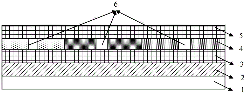
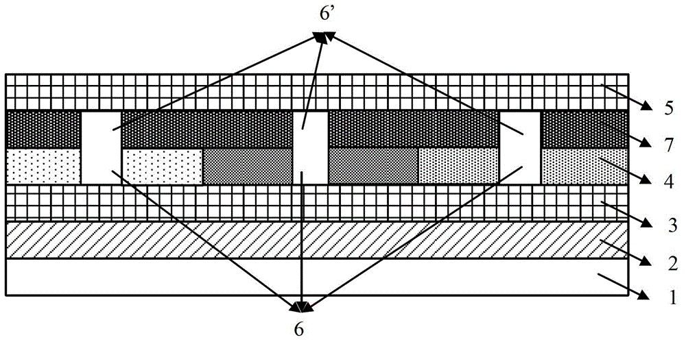
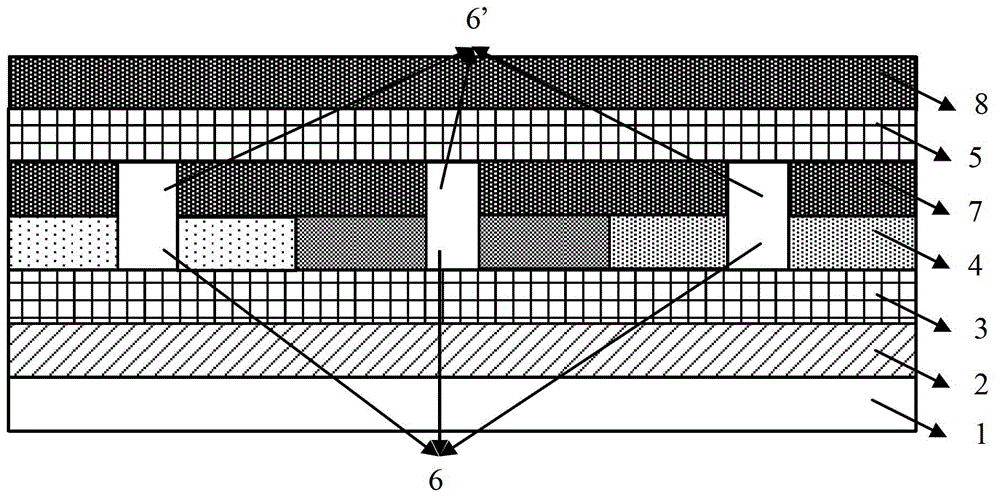
[0025] In order to solve the problems of low signal-to-noise ratio, high power consumption, and poor picture quality of the embedded touch display panel in the prior art. In the embodiment of the present invention, the first insulating layer is added between the RGB color resist layer and the second conductive film layer in the color filter substrate, thereby increasing the distance between the first conductive film layer and the second conductive film layer, This structure effectively reduces the parasitic capacitance of the color filter substrate, and improves the signal-to-noise ratio of the in-cell touch function display panel using the color filter substrate; and, during the production process of the color filter substrate, the first insulating layer can effectively Block the damage to the RGB color-resist layer caused by conductive substances and photoresist stripping solution when making the second conductive film layer, so that there is no color difference and damage in...


PUM

PropertyMeasurementUnit
thicknessaaaaaaaaaa

Abstract

The invention discloses a color film substrate, a manufacturing method of the same and a display panel. The color film substrate comprises a substrate, a first conducting film layer formed on the substrate, an RGB (Red Green Blue) color barrier layer formed on the first conducting film layer, a first insulating layer formed on the RGB color barrier layer, a second conducting film layer formed on the first insulating layer, and the RGB color barrier layer and the first insulating layer are provided with via holes. According to the color film substrate, the manufacturing method of the same and the display panel, the distance between the first conducting film layer and the second conducting film layer is enlarged, so that the parasitic capacitance of the color film substrate can be effectively reduced and the signal to noise ratio of a built-in touch function display panel with the color film substrate can be improved; further, in the manufacturing process of the color film substrate, the first insulating layer can effectively prevent the damage to the RGB color barrier layer from conductive materials and photoresist stripping liquid during the manufacturing of the second conducting film layer so as to ensure the picture display quality of the built-in touch function display panel with the color film substrate.

Description

technical field [0001] The invention relates to the field of display panel manufacture, in particular to a color filter substrate, a manufacturing method thereof, and a display panel. Background technique [0002] At present, the color filter substrate of an in-cell touch function display panel usually includes a substrate 1, a black matrix 2, a first conductive film layer 3, an RGB color resistance layer 4, and a second conductive film layer 5, wherein: [0003] The black matrix 2 is located on the substrate 1 ; the first conductive film layer 3 is located on the black matrix 2 ; the RGB color resist layer 4 is located on the first conductive film layer 3 ; the second conductive film layer 5 is located on the RGB color resist layer 4 . [0004] refer to figure 1 It can be seen from the schematic structural diagram of the color filter substrate shown that the RGB color-resist layer 4 is located between the first conductive film layer 3 and the second conductive film layer 5...

Claims


Application Information

Patent Timeline
Patent Type & Authority Applications(China)
IPC IPC(8): G02F1/1335G02F1/133G02F1/1333G06F3/041
CPCG02F1/13338G02F1/133514G02F2201/121G02B5/201
Inventor 卢峰马骏曾章和
Owner SHANGHAI TIANMA MICRO ELECTRONICS CO LTD
Why Eureka
Try Eureka