High efficiency FinFET diode

A gate structure, semiconductor technology, applied in the direction of semiconductor/solid-state device components, semiconductor devices, electrical components, etc., can solve the problems of reducing diode efficiency, reducing diode efficiency, reducing the effective area of ​​injection current, etc.

Active Publication Date: 2014-07-09
TAIWAN SEMICON MFG CO LTD
View PDF4 Cites 16 Cited by
  • Summary
  • Abstract
  • Description
  • Claims
  • Application Information

AI Technical Summary

Problems solved by technology

However, diodes constructed using FinFET structures have the disadvantage of reduced efficiency compared to conventional planar semiconductor diodes due to degradation caused by the fin structure
The presence of multiple fin structures in a FinFET diode reduces the effective area used to generate the injection current, thereby reducing the diode efficiency determined by the injection current generated per unit cell area

Method used


Image

  • High efficiency FinFET diode
  • High efficiency FinFET diode
  • High efficiency FinFET diode

Examples


Embodiment Construction

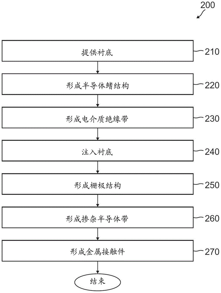
[0034] It should be understood that the invention provides many different embodiments or examples for implementing different features of the invention. Specific examples of components and arrangements are described below to simplify the present disclosure. Of course, these are examples only and are not intended to be limiting. For example, in the following description, a first component formed over or on a second component may include an embodiment in which the first component and the second component are formed in direct contact, and may also include an embodiment in which the first component and the second component are formed in direct contact. Embodiments of other components are formed between the components, that is, embodiments in which the first component and the second component are not in direct contact. In addition, the present invention may repeat reference numerals and / or letters in various instances. This repetition is intended for brevity and clarity, and by it...


PUM


Abstract

Disclosed are a FinFET diode of high efficiency, designed to resolve the degradation problem with a conventional FinFET diode arising from reduced active area, and a method of fabrication. The FinFET diode has a doped substrate, two spaced-apart groups of substantially parallel, equally-spaced, elongated semiconductor fin structures, dielectric layers formed between the two groups and among the fin structures for insulation, a plurality of substantially equal-spaced and parallel elongated gate structures perpendicularly traversing both groups of the fin structures, and two groups of semiconductor strips respectively formed lengthwise upon the two groups of the fin structures. The two groups of semiconductor strips are doped to have opposite conductivity types, p-type and n-type. The FinFET diode further has metal contacts formed upon the semiconductor strips. In an embodiment, the semiconductor strips may be integrally formed with the fin structures by epitaxial growth and in-situ doped.

Description

[0001] This application claims priority to US Provisional Patent Application Serial No. 61 / 747,764, filed December 31, 2012, the entire contents of which are hereby incorporated by reference. technical field [0002] The present invention relates generally to the field of semiconductors, and more particularly to high efficiency FinFET diodes. Background technique [0003] The semiconductor industry has evolved to pursue higher device density, higher performance, and lower cost nanotechnology nodes. As such advances have occurred, the challenges of fabrication and design issues have prompted the development of three-dimensional designs, such as Fin Field Effect Transistor (FinFET) devices. The use of FinFET devices has gained popularity in the semiconductor industry. FinFET devices offer several advantages over traditional metal-oxide-semiconductor field-effect transistor (MOSFET) devices, also known as planar devices. These advantages may include higher chip area efficienc...

Claims


Application Information

Patent Timeline
Patent Type & Authority Applications(China)
IPC IPC(8): H01L29/41H01L29/861
CPCH01L29/66136H01L29/861H01L29/161H01L29/1608H01L29/201H01L27/0924H01L21/823821H01L21/326H01L23/60H01L29/78H01L29/7848H01L21/823814H01L29/165H01L21/0257H01L21/26513H01L21/823871H01L21/823878
Inventor 范学实张胜杰胡嘉欣梁铭彰吴显扬谢文兴黄靖方
Owner TAIWAN SEMICON MFG CO LTD
Why Eureka
Try Eureka