Eureka AIR delivers breakthrough ideas for toughest innovation challenges, trusted by R&D personnel around the world.

A kind of preparation method of electronic device or circuit diagram

A technology of electronic devices and circuit diagrams, which is applied in the manufacture of printed circuits, electrical components, printed circuits, etc., can solve the problems of high ink adhesion, increased production costs, and pattern deviation, achieving low cost, saving time, and improving The effect of work efficiency

Active Publication Date: 2017-02-15
CHENGDU SCI & TECH DEV CENT CHINA ACAD OF ENG PHYSICS +1
View PDF4 Cites 0 Cited by
  • Summary
  • Abstract
  • Description
  • Claims
  • Application Information

AI Technical Summary

Problems solved by technology

[0003] 1. Since liquid ink usually contains organic solvents such as isopropanol, propyl acetate, and ethyl acetate, such organic solvents always exist in the process of printing electronic devices, and long-term contact with organic solvents is harmful to technology. The personnel's skin, central nervous system, respiratory system and other organs will cause certain damage
[0004] 2. Since the liquid ink adheres to the substrate has a certain degree of diffusion, the degree of diffusion will be affected by the characteristics of the ink itself and the condition of the substrate surface, which will cause a certain deviation between the printed pattern and the original design pattern
[0005] 3. In the existing electronic printing technology, the liquid ink must be attached to the substrate, which requires a high degree of adhesion of the ink. Therefore, it is usually required to carry out necessary chemical treatment on the surface of the substrate, which undoubtedly increases production. cost

Method used


Image

  • A kind of preparation method of electronic device or circuit diagram
  • A kind of preparation method of electronic device or circuit diagram
  • A kind of preparation method of electronic device or circuit diagram

Examples


Embodiment

[0031] Embodiment: metal palladium is used as catalyst particles, polystyrene is used as fixing agent particles to prepare electronic device method

[0032] Prepare the mixture of catalyst particles and fixative particles: metal palladium and polystyrene are ground into fine particles by ball mill respectively, wherein the particle diameter of metal palladium after grinding is 10nm (here metal palladium can be 1nm after grinding. to 1mm), polystyrene is ground into small particles with a particle size of 1um (wherein the particle size of polystyrene particles after grinding can range from 0.1um to 10um), then the small metal palladium and and The polystyrene is mixed according to the specific gravity of 100:5, and the mixture is placed in a device, and the device can charge the above mixture.

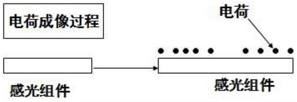
[0033] Imaging on photosensitive components: such as figure 1 As shown, the pattern of the electronic device or circuit diagram that needs to be prepared is drawn on the computer, and ...


PUM


Abstract

The invention discloses a manufacturing method of an electronic device or a circuit diagram. In the method, catalyst granules and fixing agent granules are mixed according to a certain ratio, mixtures of the catalyst granules and the fixing agent granules are applied to a flexible substrate by means of the electric charge imaging principle, and the required electronic device or the required circuit diagram is obtained in a metal chemical sedimentation method. In the method, as the solid catalyst granules are used, a pattern is applied to the substrate, and accuracy is high; in addition, efficiency is high and an application range is wide when the method is used for manufacturing the electronic device or the circuit diagram.

Description

technical field [0001] The invention relates to the field of manufacturing electronic components, in particular to a method for preparing electronic devices or circuit diagrams by using catalyst particles. Background technique [0002] According to the current situation in the field of electronic device manufacturing in my country, at present, there is no new technology that directly immobilizes solid catalyst particles on the substrate, and then obtains electronic devices or circuit diagrams, which is similar to the printing technology of electronic devices, through chemical deposition of metal ions. . We know that electronic printing technology has played an increasingly important role in the field of electronic device manufacturing. This technology can effectively reduce production costs and process complexity, and can prepare electronic structures with more superior performance and environmental sustainable development requirements. The existing electronic printing techn...

Claims


Application Information

Patent Timeline
Patent Type & Authority Patents(China)
IPC IPC(8): H05K3/18
Inventor 刘禹杨军王晓龙张腾元刘焕明梅军
Owner CHENGDU SCI & TECH DEV CENT CHINA ACAD OF ENG PHYSICS
Why Eureka
Eureka Blog
Learn More