A kind of laser pulse annealing method

A laser pulse annealing and pulse technology, which is applied in laser welding equipment, electrical components, circuits, etc., can solve the problems of difficulty in meeting the thermal budget and low efficiency, and achieve the effect of improving annealing efficiency

Active Publication Date: 2015-11-25
SHANGHAI HUALI MICROELECTRONICS CORP
View PDF6 Cites 0 Cited by
  • Summary
  • Abstract
  • Description
  • Claims
  • Application Information

AI Technical Summary

Problems solved by technology

[0008] The purpose of the present invention is to overcome the above-mentioned low efficiency caused by the single wafer annealing process in the prior art, and it is difficult to meet the increasingly stringent demand for thermal budget, and to provide a new type of laser pulse annealing equipment, which can The laser pulse annealing method for batch annealing of wafers changes the design of the wafer fixing device set in the reaction chamber of the laser pulse annealing equipment from a form that can only place a single wafer to a disc form, which is designed around the circumference of the disc. There are several wafer placement grooves, and the disk can rotate and move linearly, so that the wafers in each wafer placement groove can cycle through the laser irradiation point in turn under the continuous rotation and linear reciprocating movement of the disk. Receive uniform laser irradiation to realize batch annealing of wafers

Method used


Image

  • A kind of laser pulse annealing method
  • A kind of laser pulse annealing method
  • A kind of laser pulse annealing method

Examples


Embodiment Construction

[0029] The specific embodiment of the present invention will be further described in detail below in conjunction with the accompanying drawings.

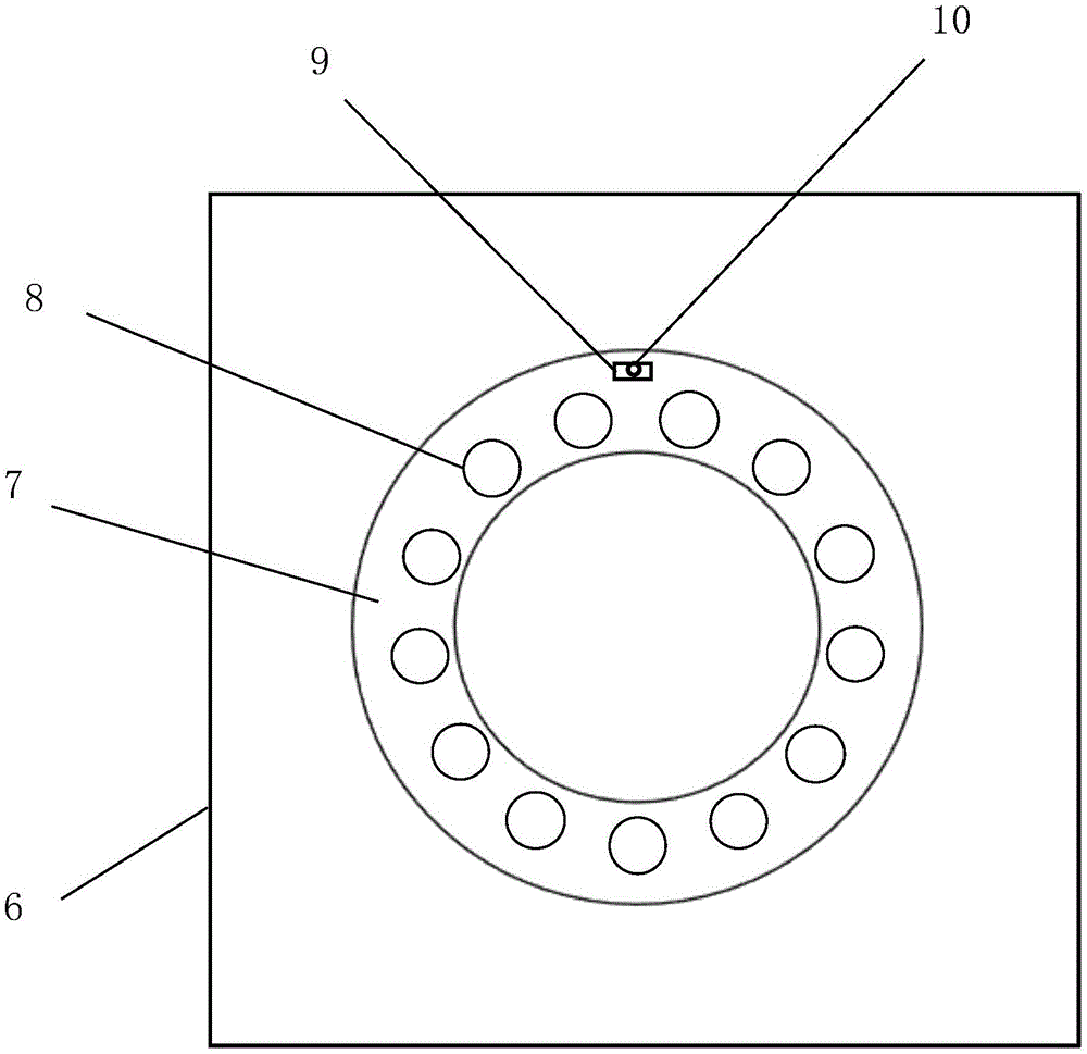
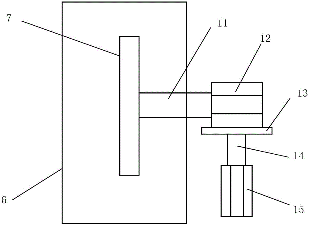
[0030] In this embodiment, firstly, the structure of the equipment used in the laser pulse annealing method of the present invention is introduced in detail. see figure 2 , figure 2 It is a schematic diagram of the front view structure of the equipment reaction chamber used in the laser pulse annealing method of the present invention. As shown in the figure, in the present invention, a disk 7 for placing a wafer is arranged in a vertical state in the reaction chamber 6 of the laser pulse annealing device. The side of the disk 7 facing the laser transmitter of the equipment (not shown) is evenly provided with 13 wafer placement grooves 8 around the circumference of the disk 7, and a 300mm wafer can be fixedly placed in each groove. The groove 8 can use a bayonet or a chuck to fix the wafer. The pulsed laser beam emitted by the ...


PUM


Abstract

The invention discloses laser pulse annealing equipment and an annealing method applied to the laser pulse annealing equipment. A disk in which multiple wafers can be simultaneously placed is arranged in a reaction cavity of the laser pulse annealing equipment and is made to rotate and linearly move in the annealing treatment process, so that the wafers in wafer placement grooves in the disk sequentially and circularly pass through laser radiation points to be uniformly radiated by laser under driving of continuous rotation and linear reciprocating motion of the disk, and bulk annealing treatment on the wafers is achieved. According to the laser pulse annealing equipment and the annealing method, compared with traditional laser pulse annealing equipment which can only carry out annealing treatment on a single wafer, the laser pulse annealing equipment has the same annealing effect, annealing efficiency is remarkably improved, and the equipment and the method can well meet the process demands for annealing quality and efficiency in the high-end advanced process.

Description

technical field [0001] The invention relates to a laser pulse annealing device for semiconductor processing, more specifically, to a laser pulse annealing device capable of performing batch annealing on semiconductor wafers and an annealing method using the device. Background technique [0002] In the manufacture of semiconductor integrated circuits, according to different processes, such as including (but not limited to) chemical vapor deposition, oxidation or nitriding, ion implantation annealing, and doping activation, it is often necessary to perform multi-step annealing on the wafer. Heat treatment repairs crystal damage and eliminates dislocations. Currently, these heat treatments can be carried out, for example, in conventional vertical furnace installations. Although the process time required for these heat treatments may be relatively short, the heating and cooling rates of conventional equipment such as vertical furnaces are relatively slow. The longer times duri...

Claims


Application Information

Patent Timeline
Patent Type & Authority Patents(China)
IPC IPC(8): B23K26/08H01L21/67H01L21/268
CPCH01L21/268H01L21/324H01L21/67115H01L21/68771H01L21/68785
Inventor 董琪琪谢威赖朝荣苏俊铭
Owner SHANGHAI HUALI MICROELECTRONICS CORP
Why Eureka
Try Eureka