Semiconductor annealing method, annealing device and annealing system

An annealing device and semiconductor technology, applied in semiconductor/solid-state device manufacturing, chemical instruments and methods, crystal growth, etc., can solve problems such as damage and reduction of surface elements or protective layers, improve annealing treatment efficiency, and reduce annealing treatment temperature. Effect

Pending Publication Date: 2022-07-29
JIHUA LAB
View PDF0 Cites 0 Cited by
  • Summary
  • Abstract
  • Description
  • Claims
  • Application Information

AI Technical Summary

Problems solved by technology

[0004] The purpose of this application is to provide a semiconductor annealing method, annealing device and annealing system, which can reduce the annealing temperature and improve the annealing efficiency while ensuring the annealing effect, and solve the problem of the surface elements or protection of SiC semiconductor sheets. layer damage

Method used


Image

  • Semiconductor annealing method, annealing device and annealing system
  • Semiconductor annealing method, annealing device and annealing system
  • Semiconductor annealing method, annealing device and annealing system

Examples


Embodiment 1

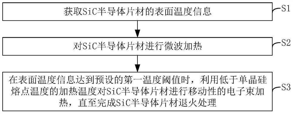
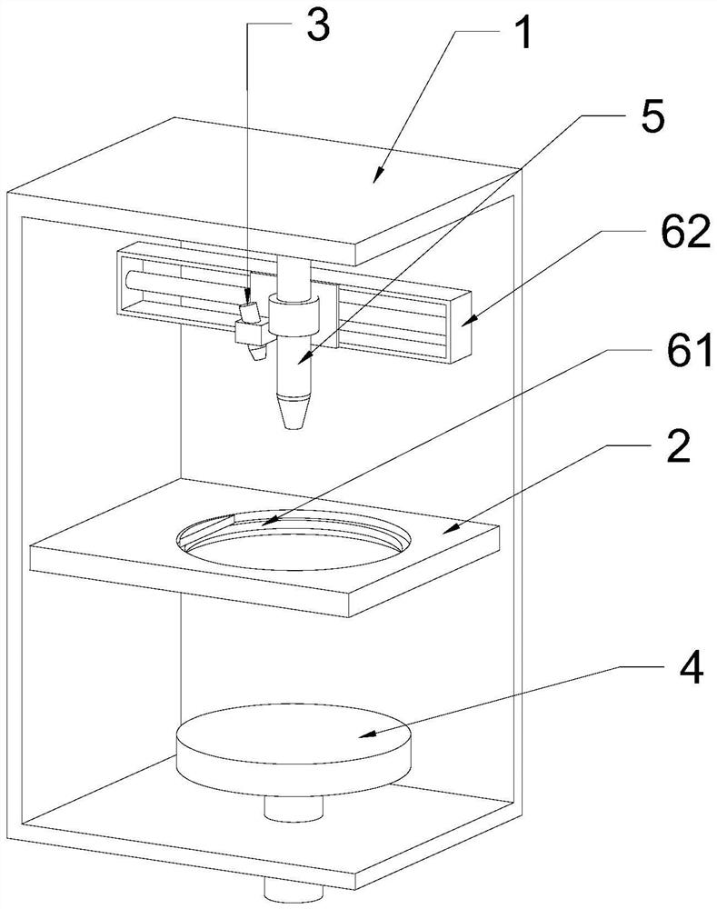
[0136] In order to more clearly illustrate the embodiments of the present application, Image 6 The semiconductor annealing apparatus shown anneals the SiC semiconductor sheet (hereinafter referred to as SiC sheet) produced by ion implantation of SiC, and the process is as follows:

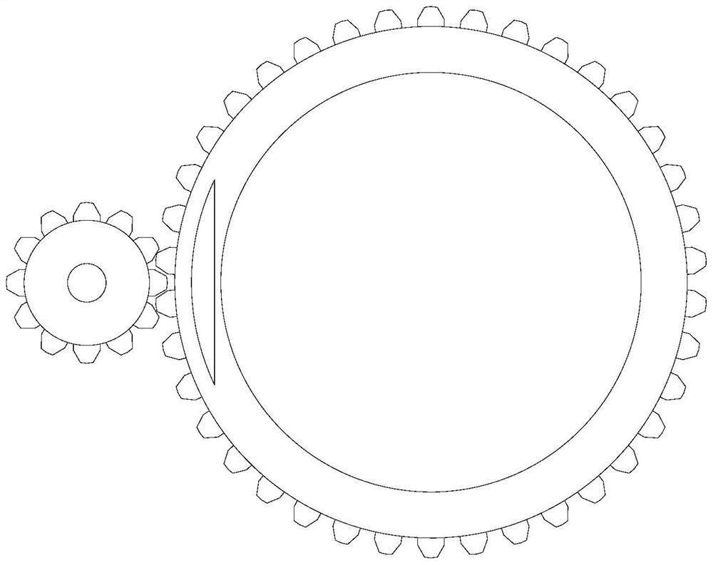
[0137] After both the loading chamber 7 and the annealing chamber 1 are filled with protective gas, the SiC chip is moved to the supporting mechanism 2 by the loading and unloading manipulator 8, and the controller 9 controls the first rotating component 61 and the microwave heating mechanism 4 to start, so that the SiC chip is activated Continue to rotate, and use the microwave heating mechanism 4 to microwave the SiC sheet. The microwave frequency of the microwave heating mechanism 4 is 2.45 GHz. The ion implantation type, ion implantation degree and thickness of the SiC sheet will affect the efficiency of microwave heating.

[0138] During the microwave heating process, the surface temperature ...


PUM

PropertyMeasurementUnit
melting pointaaaaaaaaaa

Abstract

The invention relates to the technical field of semiconductor device preparation, and particularly discloses a semiconductor annealing method, an annealing device and an annealing system.The method comprises the following steps that surface temperature information of a SiC semiconductor sheet is obtained; performing microwave heating on the SiC semiconductor sheet at a heating temperature lower than the melting point temperature of the monocrystalline silicon; when the surface temperature information reaches a preset first temperature threshold value, movable electron beam heating is conducted on the SiC semiconductor sheet till annealing treatment of the SiC semiconductor sheet is completed; according to the method, the SiC semiconductor sheet is heated to the first temperature threshold value through microwave heating treatment, the temperature needed by annealing treatment of the SiC semiconductor sheet can be reduced to be within the expected range, then accurate temperature control annealing treatment is conducted on the SiC semiconductor sheet through electron beam heating, and the temperature of the SiC semiconductor sheet can be reduced under the condition that the annealing treatment effect is guaranteed. The annealing treatment temperature is reduced, and the annealing treatment efficiency is improved.

Description

technical field [0001] The present application relates to the technical field of semiconductor device preparation, and in particular, to a semiconductor annealing method, an annealing apparatus, and an annealing system. Background technique [0002] In the prior art, after the semiconductor sheet is prepared, it needs to be annealed, but its annealing temperature is relatively high, which is easy to cause damage to its surface elements or protective layer. In other words, the rapid annealing temperature is generally above 1600 °C, the melting point of Si is 1400 °C, and the melting point of SiC is 1700 °C. Although the annealing process can activate the ions, it may lead to the volatilization of the Si element on the surface of the material and cause damage to the original SiC wafer. At present, the main method to avoid it is to coat the surface of the SiC semiconductor sheet with a protective layer. However, above 1600°C, the material of the protective layer is not stable ...

Claims


Application Information

Patent Timeline
Patent Type & Authority Applications(China)
IPC IPC(8): H01L21/263H01L21/268H01L21/324H01L21/67C30B33/02
CPCH01L21/2636H01L21/268H01L21/324H01L21/67115H01L21/67248C30B33/02
Inventor 刘欣然高桑田唐卓睿郭嘉杰何嵩吴国发
Owner JIHUA LAB
Why Eureka
Try Eureka