A kind of laser annealing apparatus and method

A technology of laser annealing and laser irradiation, which is used in the manufacture of electrical components, circuits, semiconductor/solid-state devices, etc., and can solve the problems of uneven temperature distribution and annealing effect on the surface of silicon wafers.

Active Publication Date: 2021-10-01
SHANGHAI MICRO ELECTRONICS EQUIP (GRP) CO LTD
View PDF10 Cites 0 Cited by
  • Summary
  • Abstract
  • Description
  • Claims
  • Application Information

AI Technical Summary

Problems solved by technology

[0007] The invention provides a laser annealing device and method to solve the problem of uneven temperature distribution and annealing effect on the surface of silicon wafers existing in the prior art

Method used


Image

  • A kind of laser annealing apparatus and method
  • A kind of laser annealing apparatus and method
  • A kind of laser annealing apparatus and method

Examples


Embodiment 1

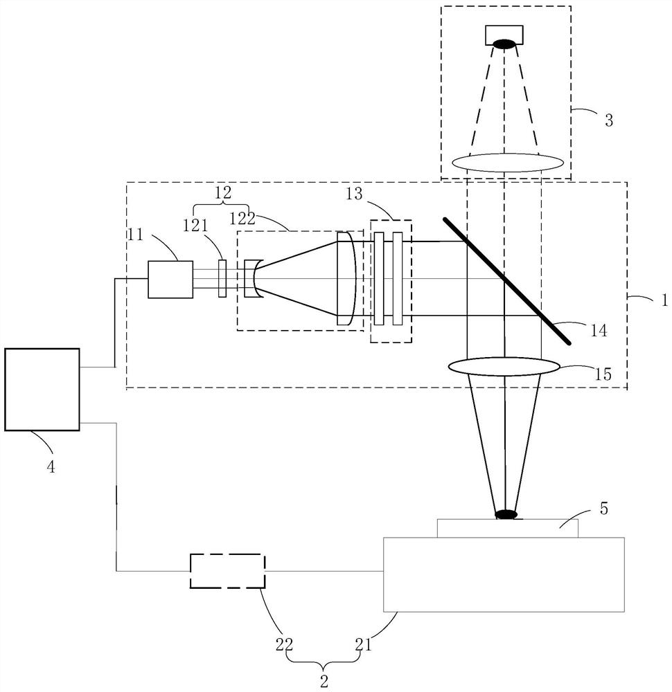
[0052] Such as image 3 As shown, the present invention provides a laser annealing device, including a laser irradiation system 1, a slide system 2, and a reflected light detection system 3 arranged sequentially along the optical path, as well as the laser irradiation system 1, the slide system 2, and the reflected light detection system. The host 4 connected to the detection system 3; the laser irradiation system 1 includes a laser light source 11, a beam adjustment component 12, a light intensity distribution forming component 13, a beam splitting component 14 and a focusing component 15 arranged sequentially along the optical path;

[0053] The laser light emitted by the laser light source 11 sequentially passes through the beam adjustment component 12, the light intensity distribution forming component 13, the beam splitting component 14 and the focusing component 15, and then projects onto the silicon wafer 5 of the slide system 2, and the reflected beam sequentially Afte...

Embodiment 2

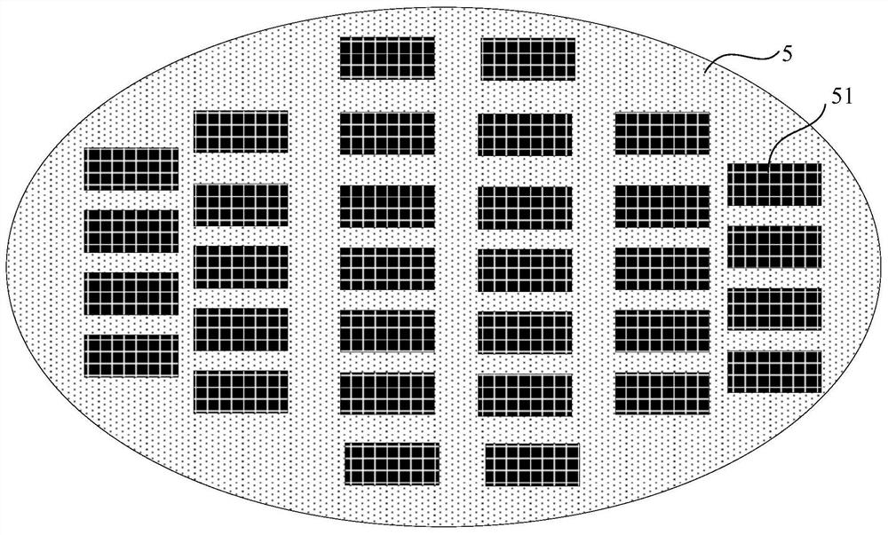
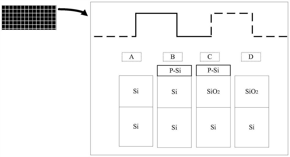
[0069] The difference from Embodiment 1 is that in this embodiment, the light intensity distribution forming assembly 13 includes a turntable 131 and a number of transmittance compensation plates or a number of mask plates (that is, mask plates with A specific transmission pattern, so that the light beam irradiated on the mask passes through the mask plate according to the specific transmission pattern to form a corresponding light intensity distribution). Specifically, the transmittance compensation plate or mask plate is customized according to the surface topography of the actual annealed silicon wafer 5, that is, the surface of the silicon wafer 5 is irradiated with a uniform laser beam, and the energy of the reflected beam detected by the reflected light detection system 3 Distributed calculation of the reflectance of the surface of the silicon wafer 5, thereby obtaining the absorptivity of the surface of the silicon wafer 5, and calculating the light intensity distributio...


PUM


Abstract

The invention discloses a laser annealing device and method. The device comprises a laser irradiation system, a slide system and a reflected light detection system sequentially arranged along the optical path, and a host computer connected with the laser irradiation system, the slide system and the reflected light detection system The laser irradiation system includes a laser light source, a beam adjustment component, a light intensity distribution forming component, a beam splitting component and a focusing component arranged in sequence along the optical path; the incident light intensity required for the silicon wafer is formed by selecting the optical elements on the light intensity distribution forming component distribution, so that the temperature field on the silicon wafer reaches the effect of consistent temperature between the middle and the edge, ensuring the uniformity of the annealing temperature, thereby improving the uniformity of the annealing effect; based on the same batch of silicon wafers, the patterns at the same position are the same, and the annealing The optical components used in the process are well selected, and the exposure process is written in order. During the exposure process, only monitoring is performed without adjustment, which can improve efficiency and increase productivity while ensuring annealing performance.

Description

technical field [0001] The invention relates to the technical field of laser annealing, in particular to a laser annealing device and method. Background technique [0002] Driven by Moore's Law, the chip manufacturing industry has experienced rapid development in the past few decades. This continued rapid development stems from the continued shrinking of chip sizes. However, as the size shrinks, more and more difficulties and challenges are raised for the chip manufacturing process, and the traditional rapid thermal annealing method of silicon wafers has been difficult to meet the requirements of 45nm and higher nodes. [0003] In recent years, due to the development of laser application technology and the advantages of smaller thermal budget and higher activation efficiency compared with traditional annealing, laser annealing can greatly reduce thermal diffusion and reduce thermal strain, and has shown a good application prospect. [0004] After the silicon wafer undergoe...

Claims


Application Information

Patent Timeline
Patent Type & Authority Patents(China)
IPC IPC(8): H01L21/324H01L21/67
CPCH01L21/324H01L21/67098
Inventor 徐建旭崔国栋兰艳平
Owner SHANGHAI MICRO ELECTRONICS EQUIP (GRP) CO LTD
Why Eureka
Try Eureka