Light emission angle modulation device for three-dimensional displayer pixels

A technology of emission angle and light source, applied in the direction of instruments, optics, optical components, etc., can solve the problem that the pixel cannot freely control the direction of light emission, etc., and achieve the effect of simple structure, easy industrialization, and good compatibility

Inactive Publication Date: 2014-07-16
JILIN UNIV
View PDF2 Cites 12 Cited by
  • Summary
  • Abstract
  • Description
  • Claims
  • Application Information

AI Technical Summary

Problems solved by technology

[0006] This patent is very different from previous patents on three-dimensional stereoscopic display, such as patents CN200610107609.4 and CN200610103070.5, etc., which are based on traditional parallax barriers, lens arrays, etc. to form two different pictures, and then combine the two pictures The emission direction of the picture is separated and incident on the left and right eyes of the person respectively, and its pixel cannot freely control the emission direction of the light

Method used


Image

  • Light emission angle modulation device for three-dimensional displayer pixels
  • Light emission angle modulation device for three-dimensional displayer pixels
  • Light emission angle modulation device for three-dimensional displayer pixels

Examples


Embodiment 1

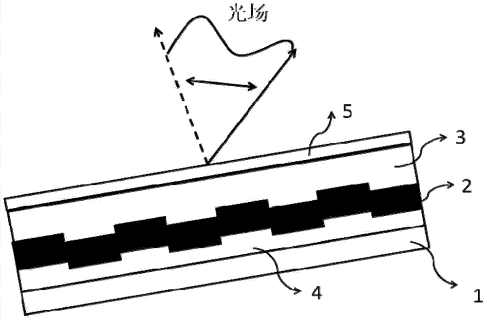
[0019] Embodiment 1: Structure of a light emission angle modulation device excited by a planar light source and modulated by surface plasmons.

[0020] like figure 1 As shown, 1 is a planar light source, and a light-emitting diode (LED) is used here with an emission wavelength of 630nm. 2 is a noble metal thin film with a nano-periodic structure, here is a thin film with a silver grating nano-periodic structure, prepared by the template method (obtained by vacuum-depositing a silver film on the strip structure on a Blu-ray disc), with a thickness of 100nm. On the upper and lower sides of the film, there are rectangular grating nano-period structures with a period of 320nm (the width of the strips is 160nm, and the spacing of the strips is 160nm) and the height is 15nm. 3 is the liquid crystal layer, here is a nematic liquid crystal (the TEB50 general-purpose liquid crystal of Hebei Chengzhi Yonghua Company), the thickness of the liquid crystal layer is 50 microns, and the ref...

Embodiment 2

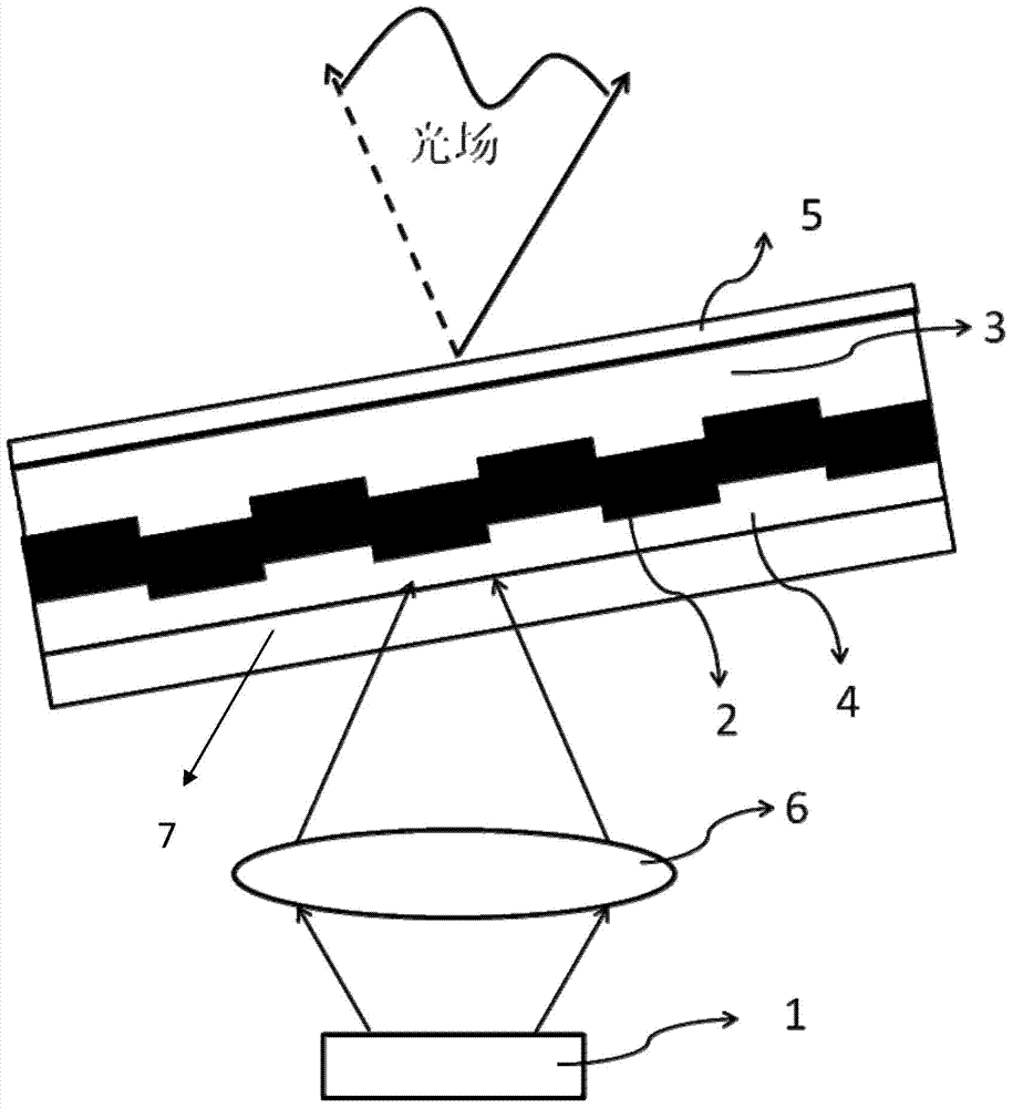
[0024] Embodiment 2: Light emission angle modulation device structure for surface plasmon modulation by focused beam illumination.

[0025] like figure 2 As shown, the difference between this embodiment and embodiment 1 is that the optical lens 6 is used to focus the monochromatic light emitted by the planar light source 1 (same as embodiment 1) onto the silver grating nano-periodic structure film 2, and the rest of the structure is the same. Since the light beam is focused, the incident angle of the silver grating nano-periodic structure thin film 2 ranges from about 0 to 30 degrees, instead of approximately -90 degrees to 90 degrees in Embodiment 1. In this way, the utilization rate of light energy is improved, and the light spots emitted by the negative level can be eliminated. But the structure is more complex than Example 1.

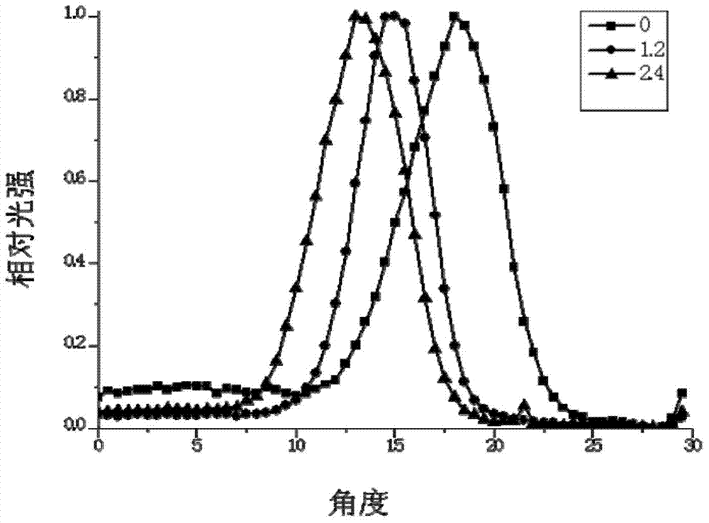
[0026] Fig. 5 is a photo of the light field distribution of the structure described in this embodiment under different electric field intensitie...


PUM


Abstract

The invention provides a light emission angle modulation device for three-dimensional displayer pixels and belongs to the technical field of naked eye three-dimensional display. The light emission angle modulation device for the three-dimensional displayer pixels is sequentially composed of a light source, a refractive index matching layer, a precious metal film, a liquid crystal layer and a transparent conducting layer, wherein the upper surface and the lower surface of the precious metal film are respectively of a nanometer period structure. Light and surface plasmons are effectively coupled on the surfaces of the precious metal film through the nanometer period structures, so that surface plasmon resonance is generated and only incident light at the surface plasmon resonance angle is made to permeate the precious metal film. The crystal liquid layer controls and adjusts the refractive index through electric signals to change the surface plasmon resonance angle, and therefore light emission angle modulation is conducted through the electric signals. According to the light emission angle modulation device, continuous scanning of the light-emitting direction and strength in a space can be achieved. A three-dimensional displayer composed through a pixel array can be used for simulation and recurrence of a scattering field of an object or different display images are projected at different angles, and therefore a three-dimensional image is displayed naturally and vividly.

Description

technical field [0001] The invention belongs to the technical field of naked-eye three-dimensional stereo display, and in particular relates to a light emission angle modulation device using surface plasmon modulation that can be used as a pixel of a three-dimensional stereo display. Background technique [0002] The principle of three-dimensional stereoscopic display is to use the difference in images observed by the left eye and the right eye of a person, that is, binocular parallax, to form a stereoscopic impression. Glasses-free three-dimensional display technology refers to the technology that can observe three-dimensional images without wearing special glasses. The existing naked-eye 3D display technology generally installs some optical devices in front of the display panel, such as parallax barriers, lens arrays, etc., to separate the images from left to right in the emission direction, so that people's left and right eyes can observe different images to form a three-...

Claims


Application Information

Patent Timeline
Patent Type & Authority Applications(China)
IPC IPC(8): G02B27/22
Inventor 徐蔚青李海波徐抒平王海谷玥娇陈刚赵冰周向华
Owner JILIN UNIV
Why Eureka
Try Eureka