TFT array substrate, display panel and display device

An array substrate and display panel technology, applied in nonlinear optics, instruments, optics, etc., can solve problems such as screen flicker and display panel crosstalk, and achieve the effects of improved balance, reduced screen flicker, and rapid current conduction

Active Publication Date: 2014-07-16
XIAMEN TIANMA MICRO ELECTRONICS +1
View PDF7 Cites 28 Cited by
  • Summary
  • Abstract
  • Description
  • Claims
  • Application Information

AI Technical Summary

Problems solved by technology

[0005] The invention provides a TFT array substrate, a display panel and a display device, so as to improve the problems of crosstalk and screen flicker of the display panel, and improve the quality of the display screen

Method used


Image

  • TFT array substrate, display panel and display device
  • TFT array substrate, display panel and display device
  • TFT array substrate, display panel and display device

Examples


Embodiment 1

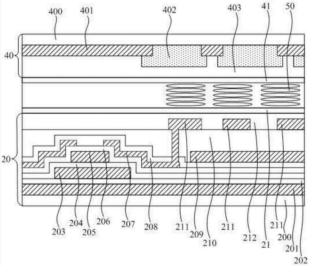
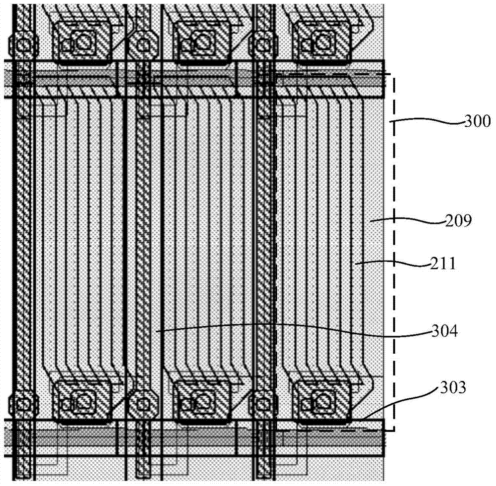
[0036] This embodiment provides a TFT array substrate, which is especially suitable for an LTPS-TFT (Low Temperature Poly-silicon Thin Film Transistor, Low Temperature Polysilicon Thin Film Transistor) array substrate. combine figure 2 , image 3 and Figure 4 As shown, among them, figure 2 A cross-sectional view of the display panel where the TFT array substrate provided in this embodiment is located, image 3 It is a top view of some pixels of the TFT array substrate provided in this embodiment, Figure 4 It is a top view of the light-shielding conductive layer of the TFT array substrate provided in this embodiment. The array substrate 20 includes: a substrate 200 , a light-shielding conductive layer 201 and a common electrode 209 . The array substrate 20 includes a plurality of pixels 300 .

[0037] The light-shielding conductive layer 201 is located on one side of the substrate 200 , and the common electrode 209 is located on a side of the light-shielding conductive ...

Embodiment 2

[0061] Based on the above-mentioned first embodiment, this embodiment provides a TFT array substrate. The array substrate further improves the large viewing angle deviation problem of the display screen on the basis of improving the screen crosstalk and flickering problems.

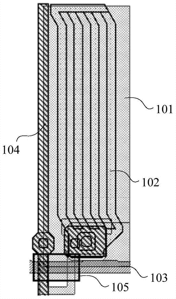
[0062] Specifically, such as Figure 5 As shown, the multiple pixels on the array substrate include red pixel R, green pixel G and blue pixel B, and the projection of the first common electrode line 303 in the direction perpendicular to the TFT array substrate intersects with the gate line. overlap, the projection of the second common electrode line 304 in the direction perpendicular to the TFT array substrate overlaps with the data line of the TFT array substrate, then the second common electrode line 304 between the red pixel R and the blue pixel B has the second common electrode line 304 a width w 1 , the second common electrode line 304 between the red pixel R and the green pixel G has a second width...

Embodiment 3

[0072] Based on Embodiment 1, this embodiment provides a TFT array substrate, such as Figure 7 As shown, along the direction of light transmission, it includes: a light-shielding conductive layer 701, a first insulating layer 702, an active layer 703, a second insulating layer 704, a gate line layer 705, a third insulating layer 706, source and drain electrodes and data lines layer 707, a fourth insulating layer 708, a common electrode layer 709, a fifth insulating layer 710, and a pixel electrode layer 711, and the TFT array substrate further includes: a first electrode ( Figure 7 not shown), the first electrode is electrically connected to the light-shielding conductive layer 701 to form a storage capacitor with the pixel electrode located on the pixel electrode layer 711 .

[0073] It can be seen from Embodiment 1 that the first common electrode line and the second common electrode line in the light-shielding conductive layer 701 are electrically connected to the common e...


PUM


Abstract

The invention provides a TFT array substrate, a display panel and a display device. The TFT array substrate comprises a base plate, a shade conducting layer, and a common electrode; the shade conducting layer is arranged on the base plate; the common electrode is arranged above the shade conducting layer. The base plate comprises a plurality of pixels. The shade conducting layer comprises shade elements, a plurality of first and second common electrode lines; the shade elements are used for shading TFT grooves in each pixel; the first common electrode lines extend in a first direction; the second common electrode lines extend in a second direction; at least one of the first and second common electrode lines is electrically connected with the common electrode; the second and first common electrode lines intersect in a mesh structure; projections of the first and second common electrode lines, perpendicular to the base plate, cover gaps among the pixels. The first and second common electrode lines forming in the mesh structure are electrically connected with the common electrode, so that voltages of the common electrode are more balanced and the problems of crosstalk and flicker are improved.

Description

technical field [0001] The present invention relates to the technical field of displays, and more specifically, to a TFT (Thin Film Transistor, Thin Film Field Effect Transistor) array substrate, a display panel and a display device. Background technique [0002] Liquid crystal display panel has many advantages such as low radiation, low power consumption, light and thin volume, etc. It is the most mainstream display panel in the field of display technology at present. Wide viewing angle is a major trend in the development of liquid crystal display panel. According to the different arrangements of liquid crystal molecules, wide viewing angle liquid crystal display panels can be divided into IPS (In-Plane Switching, in-plane switching) type, FFS (Fringe Field Switching, fringe field switching) type, VA (Vertical Alignment, vertical alignment) type . Among them, the FFS liquid crystal display panel has the advantages of high light transmittance, wide viewing angle, small cros...

Claims


Application Information

Patent Timeline
Patent Type & Authority Applications(China)
IPC IPC(8): G02F1/1343
Inventor 周秀峰
Owner XIAMEN TIANMA MICRO ELECTRONICS
Why Eureka
Try Eureka