Multi-node memory interconnection device and large-scale computer cluster

A multi-node, computer technology, applied in the direction of computers, multi-program devices, digital computer components, etc., can solve problems affecting computer performance, large resources, unfavorable maintenance and upgrade of memory devices, etc., to avoid excessive consumption of processor resources , Improving migration efficiency and shortening the data migration path

Inactive Publication Date: 2014-07-16
STACKINSIDER TECH
View PDF4 Cites 10 Cited by
  • Summary
  • Abstract
  • Description
  • Claims
  • Application Information

AI Technical Summary

Problems solved by technology

Therefore, during the data transmission process of the processor connected to the specific memory, the resources occupied by the processor are relatively large, which greatly affects the performance of the computer.
As the capacity and frequency of the computer memory system increase, the resulting technical problems will become more and more obvious, resulting in relatively low data migration efficiency between memory devices in computers in the prior art, which is not conducive to memory Equipment maintenance and upgrade

Method used


Image

  • Multi-node memory interconnection device and large-scale computer cluster
  • Multi-node memory interconnection device and large-scale computer cluster
  • Multi-node memory interconnection device and large-scale computer cluster

Examples


Embodiment 1

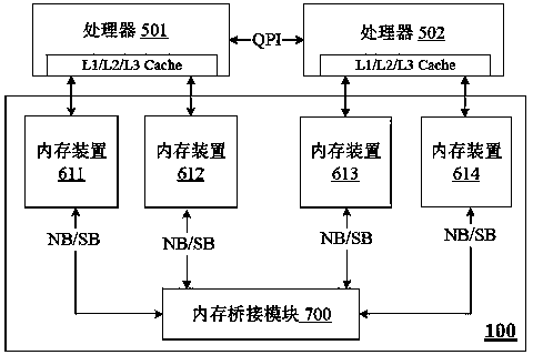
[0043] Please refer to figure 2 , image 3 , Figure 6 , Figure 9 with Figure 10 A specific implementation manner of a multi-node memory interconnection device of the present invention is shown.

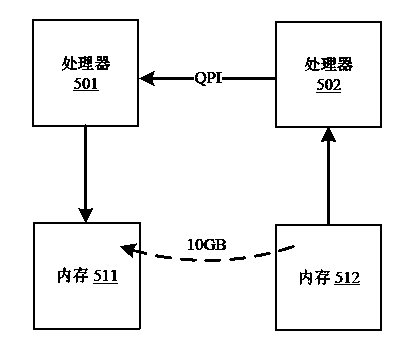
[0044] In this embodiment, the multi-node memory interconnection device 100 includes four memory devices 611 , 612 , 613 , 614 connected to the designated processors 501 , 502 . It should be noted that this embodiment is only an illustration, and the number of processors and memory devices is not limited during actual application.

[0045] Meanwhile, for ease of illustration, in this embodiment, the processor 501 is connected to the memory devices 611 and 612 in series, and the processor 502 is connected to the memory devices 613 and 614 in series.

[0046] In this embodiment, the memory devices 611 , 612 , 613 , and 614 are preferably non-volatile memory devices. It should be noted that, part or all of the memory devices 611, 612, 613, 614 can also be selected as common vol...

Embodiment 2

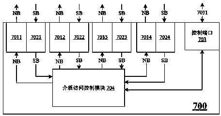
[0066] Please refer to Figure 4 Another specific implementation manner of a multi-node memory interconnection device of the present invention is shown. The main difference between this embodiment and Embodiment 1 is that in this embodiment, the multi-node memory interconnection device 100 also includes an external data sending port 7111 and an external data receiving port 7211 connected to the media access control module 704, and through the Data migration between the protocol analysis module 705 and the communication port 706 and the external computer.

[0067]Specifically, in this embodiment, the protocol analysis module 705 is selected from a WiFi analysis module. Meanwhile, the system bus 7031 is a PCI-e protocol bus. PCI-e is a high-speed serial point-to-point dual-channel high-speed broadband transmission bus form, including PCI-e X1\X2\X4\X8\X16; it can choose a specific PCI according to the storage scale of the entire multi-node memory interconnection device 100 -e...

Embodiment 3

[0070] Please refer to figure 2 , Figure 5 , Figure 7 with Figure 8 The third specific implementation manner of a multi-node memory interconnection device of the present invention is shown.

[0071] When the computer is turned on, the firmware will perform memory detection to obtain the physical address range (including the start address and end address) and port information of each memory device 611, 612, 613, 614, and generate such as Figure 5 The shown port mapping table is then sent to the memory bridge module 700 through the control port 703 . For example: when a memory device 611 with a memory capacity of 64 GB is plugged into the first SMI slot on the motherboard, the physical address range of the memory device 611 is 0x0000000000000000~0x0000000FFFFFFFF, and the port number is 0; the physical address of the memory device 612 The range is 0x0000001000000000~0x0000001FFFFFFFF, the port number is 1; the physical address range of the memory device 613 is 0x0000002...


PUM


Abstract

The invention belongs to the technical field of computer memory data transmission and provides a multi-node memory interconnection device and a large-scale computer cluster. The multi-node memory interconnection device comprises multiple memory devices connected with appointed processors and further comprises a memory bridge connection module connected with the memory devices in a coupled mode, and the memory bridge connection module comprises multiple transmitting ports, receiving ports and a control port communicating with the processors through system buses. The control port receives a port mapping table generated in the process of computer starting self-checking, and a data link is established between two or more appointed memory devices through the transmitting ports and the receiving ports according to a memory data migration operation instruction transmitted by the processors. Through the multi-node memory interconnection device, loads, on the processors, of memory data migration are avoided, processor resources are saved, the data migration route is shortened, and the efficiency of memory data migration is improved.

Description

technical field [0001] The present invention relates to the technical field of computer and internal and external memory data transmission of the computer, in particular to a multi-node memory interconnection device and a large-scale computer cluster based on the multi-node memory interconnection device. Background technique [0002] With the advent of the era of big data, higher data computing, processing, transmission, storage and other requirements are put forward for computers. Therefore, a plurality of processors (CPUs) are usually arranged on a motherboard of a server or a high-performance computer. [0003] The memory access mechanism and architecture have a decisive impact on the computing speed of the processor. In the traditional motherboard architecture, memory control is performed by the Northbridge chip, which acts as a memory control hub (MCH). A single processor can use most of the memory when performing floating-point operations, but since the use of memory...

Claims


Application Information

Patent Timeline
Patent Type & Authority Applications(China)
IPC IPC(8): G06F9/50G06F15/173
Inventor 江韬H·F·黄李惊雷
Owner STACKINSIDER TECH
Why Eureka
Try Eureka