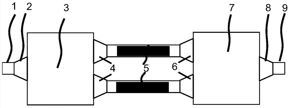
Silicon dioxide and polymer combined and integrated optical waveguide type thermal-optical modulator
A thermo-optic modulator, silicon dioxide technology, applied in instruments, optics, nonlinear optics, etc., can solve the problems of large device size and high power, and achieve the effects of small transmission loss, simple manufacturing process, and reduced coupling loss.
- Summary
- Abstract
- Description
- Claims
- Application Information
AI Technical Summary
Problems solved by technology
Method used
Image
Examples
Embodiment 1
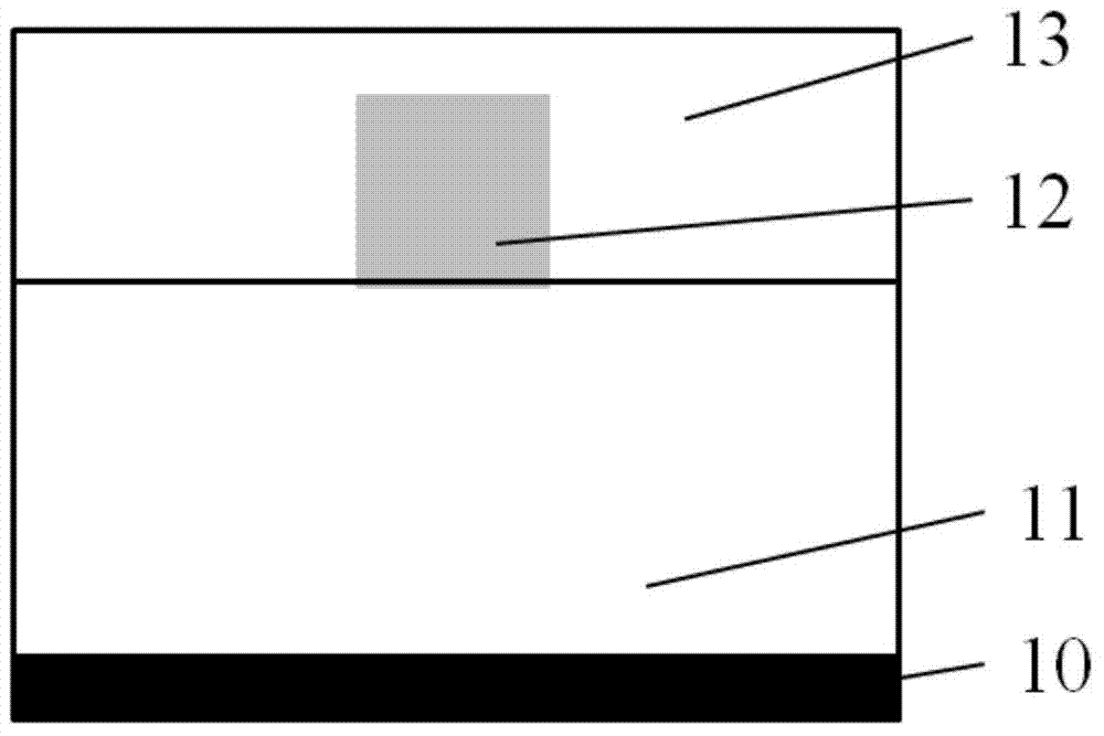
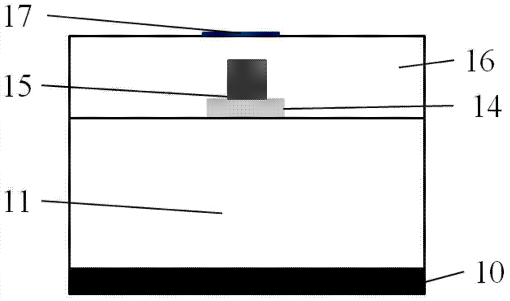
[0033] In this example, the refractive index of the silicon dioxide lower cladding layer 7 is 1.45, and the thickness is about 12 μm; the refractive index of the germanium-doped silicon dioxide core layer 8 is 1.46, and the thickness is 6 μm; the refractive index of the silicon dioxide upper cladding layer 9 is It is 1.45 and the thickness is about 4 μm. For the silicon dioxide input waveguide 1 and the silicon dioxide output waveguide 9, the height of the germanium-doped silicon dioxide core layer is 6 μm. The specific manufacturing process is as follows: a silicon dioxide lower cladding layer with a refractive index of 1.45 and a germanium-doped silicon dioxide core with a refractive index of 1.46 are sequentially deposited on a silicon substrate by plasma enhanced chemical vapor deposition (PECVD). layer. Since the refractive index 3.45 of Si is higher than that of germanium-doped silicon dioxide, the thickness of the lower cladding layer 7 of silicon dioxide must be great...
PUM
 Abstract
Description
Claims
Application Information


