Electronic component packaging structure and electronic device

An electronic component and packaging structure technology, applied in the field of electronic component packaging structure and electronic equipment, can solve problems such as poor high-frequency EMI shielding effect, and achieve the effect of improving EMI shielding effect and reducing radiated EMI.

Active Publication Date: 2014-07-23
HUAWEI TECH CO LTD
View PDF6 Cites 15 Cited by
  • Summary
  • Abstract
  • Description
  • Claims
  • Application Information

AI Technical Summary

Problems solved by technology

[0004] In the Lid electronic component packaging structure adopted above, the low DK non-conductive glue provided between the conductive casing 5 and the substrate makes the conductive casing present high impedance relative to the substrate, and this high impedance makes the gap between the conductive casing and the substrate The gap of the non-conductive adhesive becomes a radiation str

Method used


Image

  • Electronic component packaging structure and electronic device
  • Electronic component packaging structure and electronic device
  • Electronic component packaging structure and electronic device

Examples


Embodiment 1

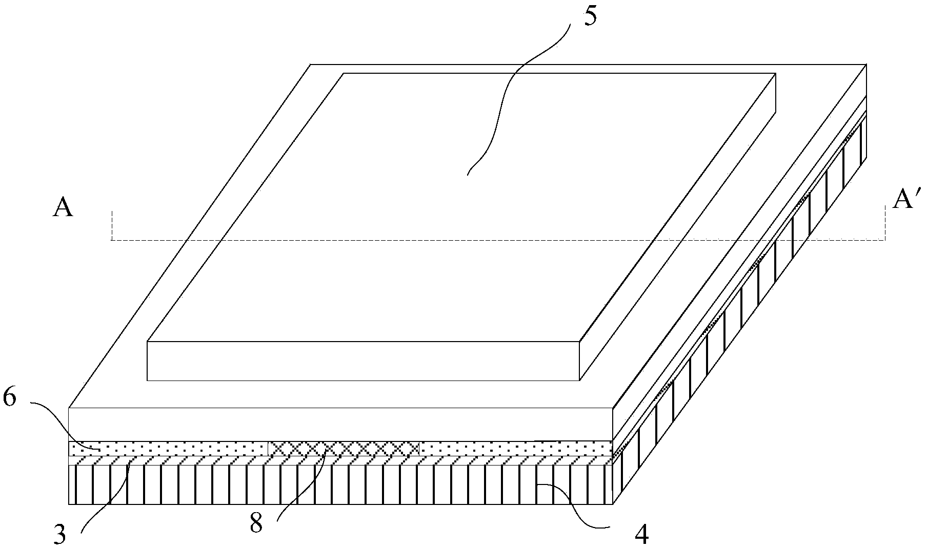
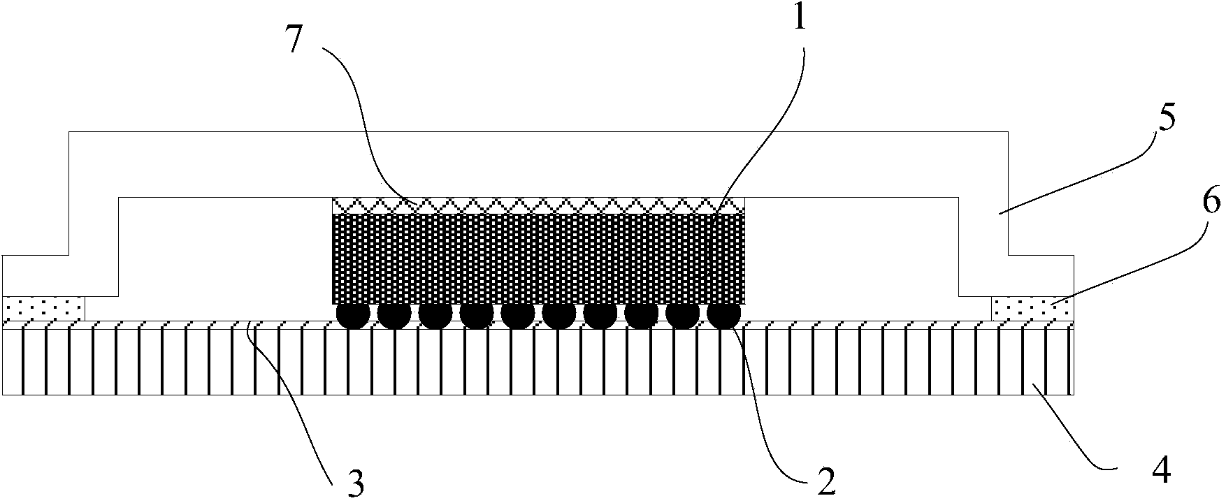
[0044] Figure 4 Shown is a top view of an electronic component packaging structure with EMI shielding effect provided by an embodiment of the present invention, Figure 5 Shown is provided by the embodiment of the present invention Figure 4 The schematic diagram of the cross-sectional structure of the packaging structure of the electronic component shown in the A-A' direction. combine Figure 4 with Figure 5 It can be seen that the electronic component packaging structure provided by the embodiment of the present invention includes an electronic component (chip or discrete component) 1, a circuit pin 2, a solder resist layer 3, a substrate 4, a conductive casing 5, and Between the non-conductive glue 6, and the thermally conductive glue 7, where:

[0045]The substrate 4 has a set attachment area S for attaching electronic components. The size and shape of the attachment area S can be set according to the size and shape of the electronic components actually packaged. 6 ...

Embodiment 2

[0061] In the embodiment of the present invention, chips can be attached in the attachment area set on the substrate 4 , and other discrete components, such as capacitors, resistors, transistors and other electronic components, can also be arranged.

[0062] The electronic component packaging structure provided in the embodiment of the present invention, the electronic component packaging structure when attaching chips, discrete components, and chips and discrete components to the attachment area set on the substrate 4 is basically the same as the above-mentioned embodiment, that is: non-conductive The adhesive has a high DK value. The coating area of ​​the high DK non-conductive adhesive on the substrate should be as large as possible, and it should be coated on the entire area of ​​the surface of the substrate facing the conductive shell except the attachment area. The thickness should be thin and the DK should be high. The removal of the solder mask layer at the non-conducti...

Embodiment 3

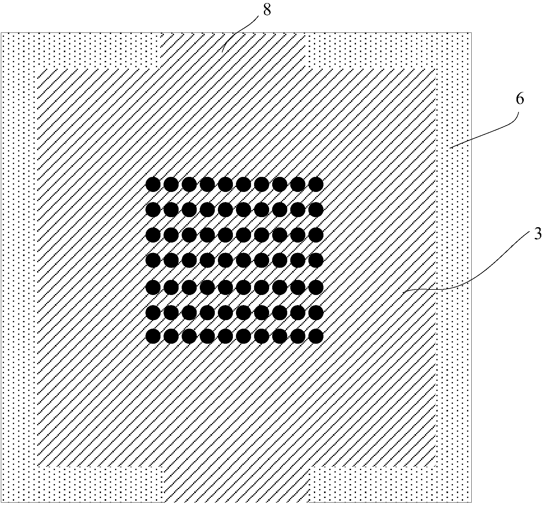
[0069] In the embodiment of the present invention, in order to ensure the reliability of the process, the vent hole 8 can be reserved on the high DK non-conductive adhesive, that is, the vent hole 8 is set on the high DK non-conductive adhesive, refer to Figure 10 with Figure 11 shown. Figure 10 Shown is a top view of the electronic component packaging structure in which the vent holes are arranged on the high DK non-conductive glue in the embodiment of the present invention, Figure 11 shown as Figure 10 The schematic diagram of the cross-sectional structure of the electronic component packaging structure shown in the A-A' direction.

[0070] Specifically, the difference between the electronic component packaging structure involved in the embodiment of the present invention and the above-mentioned embodiment lies in the setting position of the vent hole. The embodiment of the present invention will only describe the difference below, and the other same or similar points...


PUM

PropertyMeasurementUnit
Dielectric constantaaaaaaaaaa

Abstract

The invention discloses an electronic component packaging structure and an electronic device. The electronic component packaging structure at least comprises a substrate, a conductive housing and a non-conductive adhesive, wherein the substrate is provided with a set adhesion area, the set adhesion area is used for adhesion of an electronic component, the conductive housing is provided with a top and a side wall extending towards the substrate, a bonding end is arranged on the side, close to the substrate, of the side wall, the conductive housing is bonded to the substrate through the bonding end and the non-conductive adhesive, the adhesion area is surrounded by the conductive housing which is bonded to the substrate, a shielding space is formed above the adhesion area, the non-conductive adhesive is located between the substrate and the bonding end, the dielectric constant of the non-conductive adhesive is larger than or equal to seven, and the coating thickness of the non-conductive adhesive is smaller than or equal to 0.07 mm. By the adoption of the electronic component packaging structure and the electronic device, the planar capacitance density of a planar capacitance structure formed by the conductive housing, the non-conductive adhesive and the substrate is improved, then the planar capacitance value of the planar capacitance structure formed by the conductive housing, the non-conductive adhesive and the substrate can be increased, gap antenna effect radiation EMI at the position of the non-conductive adhesive can be effectively reduced, and the EMI shielding effect of the shielding space is improved.

Description

technical field [0001] The invention relates to the technical field of chip packaging, in particular to an electronic component packaging structure and electronic equipment. Background technique [0002] With the increase of chip integration and speed year by year, the high-frequency EMI (Electromagnetic Interference, electromagnetic interference) generated by the chip can easily cause various system interference and product RE (Radiation Emission, radiated emission) test exceeding the standard. [0003] At present, the packaging of chips mainly adopts Lid (flat metal packaging cover plate) electronic component packaging structure. figure 1 Shown is a top view of the chip Lid electronic component packaging structure, figure 2 shown as figure 1 The schematic diagram of the cross-sectional structure of the chip Lid electronic component packaging structure along the direction A-A' is shown. Depend on figure 1 with figure 2 It can be seen that by opening a window in the s...

Claims


Application Information

Patent Timeline
IPC IPC(8): H01L23/552H01L23/00H05K9/00
CPCH01L23/10H01L23/552H01L2224/16225H01L2224/73253H01L2924/16151H01L2924/16235H01L2924/16251H01L2924/164H01L2924/19041H01L2924/19042H01L2924/19043H01L2924/19105H05K1/0231H05K1/0236H05K1/181H05K9/0028
Inventor 虞学犬杨林白亚东
Owner HUAWEI TECH CO LTD
Why Eureka
Try Eureka