TFT array substrate, display panel and display device
An array substrate and display panel technology, which is applied in the fields of display panels, display devices, and TFT array substrates, can solve the problem of not further improving the aperture ratio, and achieve the effect of saving costs and improving the aperture ratio.
- Summary
- Abstract
- Description
- Claims
- Application Information
AI Technical Summary
Problems solved by technology
Method used
Image

Examples
Embodiment 1
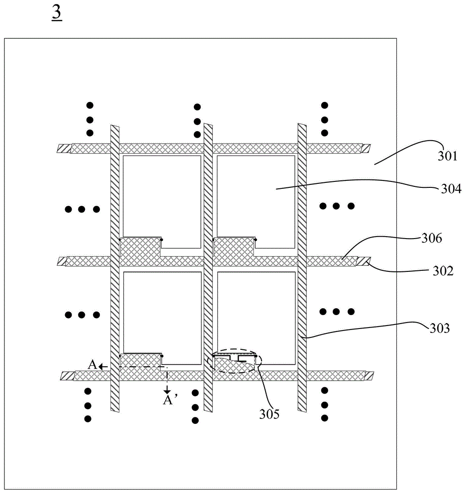
[0034] The schematic diagram of the top view structure of the TFT array substrate provided by Embodiment 1 of the present invention is as follows: image 3 As shown, the section view along A-A' is shown as Figure 4 shown.
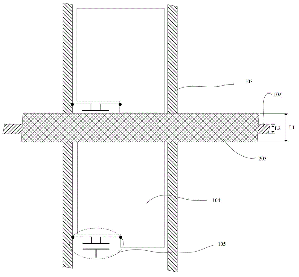
[0035] combine image 3 with Figure 4 It can be known that the TFT array substrate 3 includes a first substrate 301 and a TFT array structure layer located on the first substrate 301 . The TFT array structure layer includes a plurality of scanning lines 302; a plurality of data lines 303 insulated and intersecting with the plurality of scanning lines 302; A pixel electrode 304; a TFT 305 disposed at the intersection of the scanning line 302 and the data line 303 as a pixel switch; a high-resistance light-shielding layer 306 covering the scanning line 302 and the TFT 305. Wherein, the gate 309 of the TFT 305 is electrically connected to the corresponding scanning line 302, the source / drain 312 of the TFT 305 is electrically connected to the correspondi...
Embodiment 2
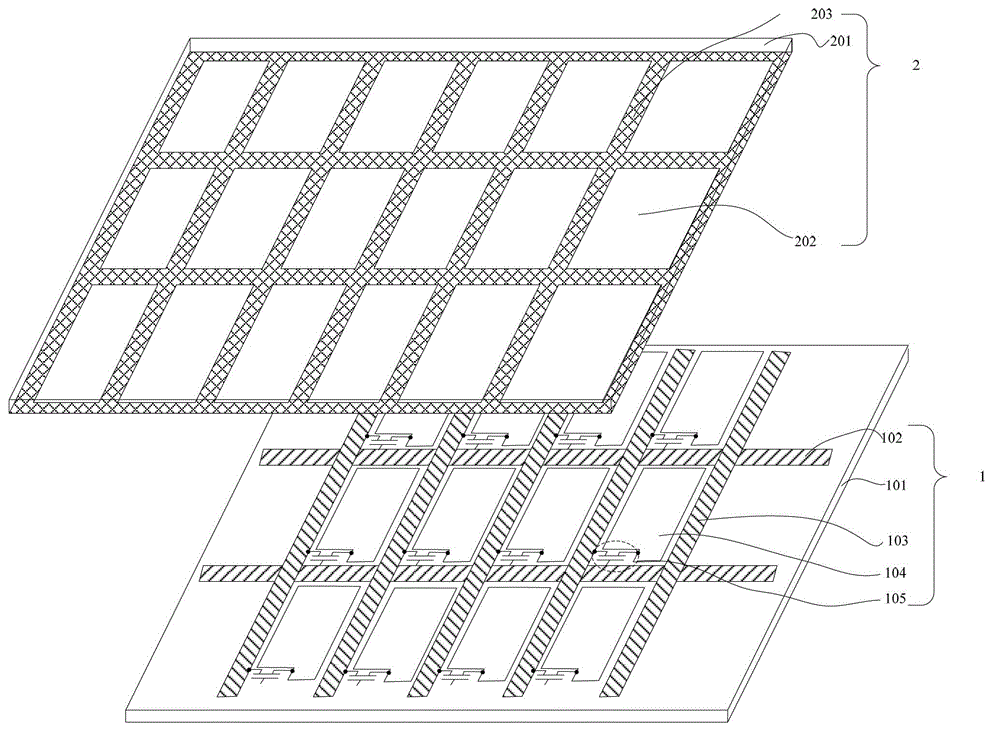
[0048] The schematic structural diagram of the display panel provided by Embodiment 2 of the present invention is as follows Image 6 shown. The display panel includes the TFT array substrate 3 described in the first embodiment and a color filter substrate 4 disposed opposite to the TFT array substrate 3 . The TFT array structure layer of the TFT array substrate 3 is located on the side of the first substrate facing the color filter substrate 4 .
[0049] The color filter substrate 4 includes a second substrate 401 ; an array of color resist units 402 and a black matrix 403 located on the side of the second substrate 401 facing the TFT array substrate 3 . The color-resist unit 402 corresponds to the pixel area of the TFT array substrate; a black matrix 403 is provided between two adjacent columns of the color-resist unit and around the edge of the second substrate 401 to shield the data line 303 . However, since the scanning lines 302 have been blocked by the light-shieldi...
Embodiment 3
[0053] The schematic structural diagram of the display panel provided by Embodiment 3 of the present invention is as follows Figure 7 shown. The display panel includes the TFT array substrate 3 described in the first embodiment and a color filter substrate 4 disposed opposite to the TFT array substrate 3 . The TFT array structure layer of the TFT array substrate 3 is located on the side of the first substrate facing the color filter substrate 4 .
[0054] The color filter substrate 4 includes a second substrate 401 ; an array of color resist units 402 located on the side of the second substrate 401 facing the TFT array substrate 3 , and an anti-reflection film 404 located on the side of the second substrate 401 facing away from the TFT array substrate 3 . The color-resist unit 402 corresponds to the pixel area of the TFT array substrate; no black matrix is arranged between adjacent color-resist units. Since the data line 303 is not blocked, light reflection will occur; ...
PUM
 Abstract
Description
Claims
Application Information
 - R&D Engineer
- R&D Manager
- IP Professional
- Industry Leading Data Capabilities
- Powerful AI technology
- Patent DNA Extraction
Browse by: Latest US Patents, China's latest patents, Technical Efficacy Thesaurus, Application Domain, Technology Topic.
© 2024 PatSnap. All rights reserved.Legal|Privacy policy|Modern Slavery Act Transparency Statement|Sitemap