Si-based field effect transistor annular terahertz detector antenna based on CMOS manufacturing process

A technology of field effect transistors and loop antennas, which is applied in the field of antenna technology and terahertz technology, and can solve problems such as limiting video rates

Inactive Publication Date: 2014-07-23
TIANJIN POLYTECHNIC UNIV
View PDF0 Cites 5 Cited by
  • Summary
  • Abstract
  • Description
  • Claims
  • Application Information

AI Technical Summary

Problems solved by technology

When these detectors are further developed into imaging equipment, there are often the following problems: first, additional processes and equipment, such as small machinery, etc. need to be added; second, the thermal relaxation time constant of the thermal effect detector limits the imaging process. rate
The THz detector based on Si-based field-effect transistor (FET) inversion layer plasma can overcome the above shortcomings, and realize THz imaging from a single CMOS field-effect transistor through a focal plane array (FPA), which has greater advantages. Domestic research in this area is still in its infancy

Method used


Image

  • Si-based field effect transistor annular terahertz detector antenna based on CMOS manufacturing process
  • Si-based field effect transistor annular terahertz detector antenna based on CMOS manufacturing process
  • Si-based field effect transistor annular terahertz detector antenna based on CMOS manufacturing process

Examples


Embodiment Construction

[0016] In order to make the objectives, technical solutions and advantages of the present invention clearer, the embodiments of the present invention will be described in further detail below in conjunction with the accompanying drawings.

[0017] In order to realize a THz detector that uses an antenna as a THz wave receiving device, a Si-based FET as a THz detection device, and a low-noise amplifier combined with a THz detector, the implementation of the present invention provides a loop antenna, which is described in detail below:

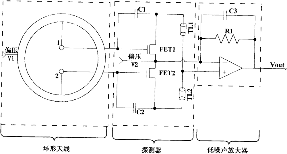
[0018] figure 1 It is a schematic diagram of a circuit structure provided by an embodiment of the present invention. Reference figure 1 The loop antenna leads out port 1 and port 2, which are respectively connected to the gates of the corresponding two FETs. At the same time, a bias voltage V2 is added to the common source of the two FETs to improve the sensitivity of the detector; the THz signal passes through the antenna After receiving, the high-fr...


PUM


Abstract

The invention discloses a Si-based FET annular THz detector antenna based on a CMOS manufacturing process, and belongs to the field of antennas. The Si-based FET annular THz detector antenna comprises an annular antenna body, a Si-based FET and a low noise amplifier. The annular antenna body is used for receiving THz waves and meanwhile converting the received THz waves into electric signals to be transmitted to the FET, high-frequency signals are converted into low-frequency signals by the FET and are transmitted to the low noise amplifier, and finally the THz signals can be detected after the signals pass through the low noise amplifier. The Si-based FET annular THz detector antenna is importantly applied to security scanning, radio astronomy, biological remote sensing, production monitoring and other fields.

Description

Technical field [0001] The present invention relates to antenna technology and terahertz technology, in particular to loop antenna technology. Background technique [0002] Terahertz (THz) waves refer to electromagnetic waves with frequencies in the range of 0.1THz to 10THz, with wavelengths in the range of 0.03mm to 3mm, between millimeter waves and infrared, which is generally considered to be the boundary area between electronics and optics. However, due to the high loss of THz waves in the air, a high-gain emission source and a sufficiently sensitive detection antenna are required, making it impossible to commercialize it in the communication field and restricting the development of technology. Therefore, this frequency band is a white space to be developed. , Also known as THz gap. [0003] THz wave has the characteristics of transient, broadband, high time and space coherence, low energy and unique transmission characteristics, making it suitable for safety monitoring, spect...

Claims


Application Information

Patent Timeline
Patent Type & Authority Applications(China)
IPC IPC(8): H01Q13/10
Inventor 李建雄李运祥蒋昊林陈晓宇刘崇袁文东
Owner TIANJIN POLYTECHNIC UNIV
Why Eureka
Try Eureka