Semiconductor package and method for manufacturing same

A manufacturing method and semiconductor technology, which are applied in the fields of semiconductor/solid-state device manufacturing, semiconductor device, semiconductor/solid-state device components, etc., can solve the problem of high wettability, reduced wiring density, and cannot fully meet the requirements of thinning And other issues

Active Publication Date: 2014-07-30
FUJI KK
View PDF5 Cites 4 Cited by
  • Summary
  • Abstract
  • Description
  • Claims
  • Application Information

AI Technical Summary

Problems solved by technology

[0008] As shown in the above-mentioned Patent Document 2, when conductive ink is ejected by a liquid droplet discharge method such as an ejector to form wiring, the wettability of ink droplets on the substrate surface (resin surface) on which the wiring is formed is high. , so the diameter of the ink droplet is large, resulting in a wide line width of the wiring, which cannot fully meet the requirements of thinning lines.
In addition, there is a disadvantage that when this wiring forming method is applied to a light-emitting element package such as an LED, the light emitted from the side surface of the light-emitting element through the transparent filling resin (base material of the wiring) is blocked by the wiring. The ratio increases, and the extraction efficiency of lig

Method used


Image

  • Semiconductor package and method for manufacturing same
  • Semiconductor package and method for manufacturing same
  • Semiconductor package and method for manufacturing same

Examples


Embodiment 1

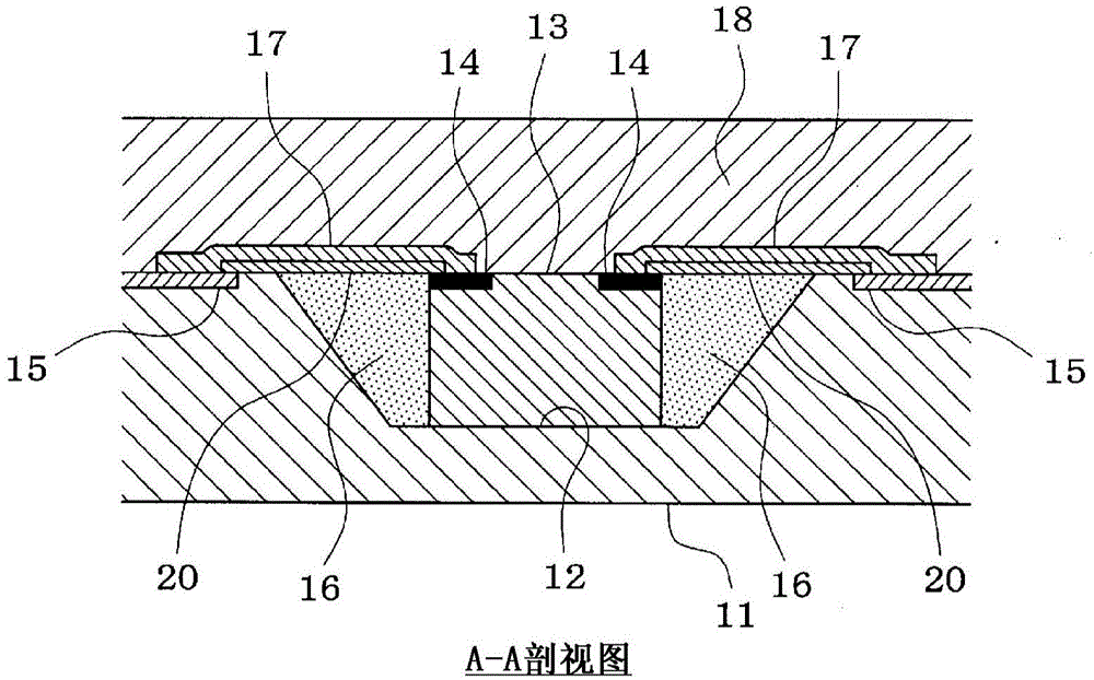
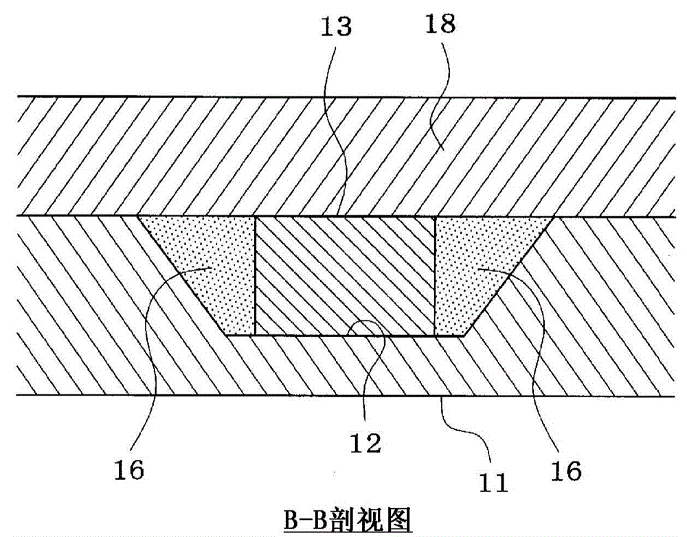
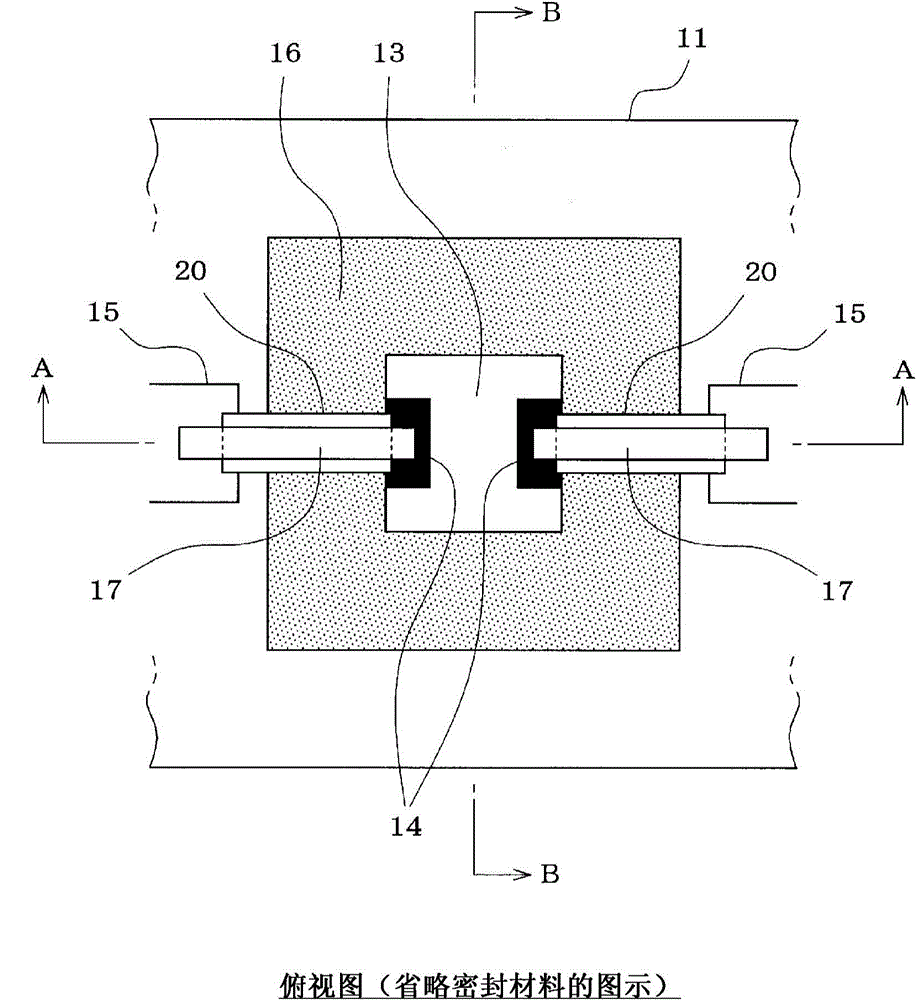
[0060] based on Figure 1 to Figure 3 Embodiment 1 of the present invention will be described.

[0061] The mounting member 11 is formed of a lead frame, a circuit board, or the like, and an element mounting recess 12 is formed at a predetermined position thereof. An LED element 13 (light emitting element) which is a semiconductor element is die-bonded (bonded) to the central portion of the bottom surface of the element mounting recess 12 of the mounting member 11 . The depth dimension (height dimension) of the element mounting recess 12 is set to be approximately the same as the height dimension of the LED element 13, and the electrode portion 14 mounted on the upper surface of the LED element 13 in the element mounting recess 12 is formed so as to be on the upper surface of the mounting member 11. The electrode parts 15 are approximately the same height.

[0062] The periphery of the LED element 13 in the element mounting recess 12 of the mounting member 11 is filled with ...

Embodiment 2

[0071] based on Figure 4 to Figure 6 Embodiment 2 of the present invention will be described.

[0072] The mounting member 30 is configured by molding a package main body 33 having an element mounting recess 32 on a lead frame 31 from resin. An LED element 34 (light emitting element) which is a semiconductor element is die-bonded (bonded) to the central portion of the bottom surface of the element mounting recess 32 of the mounting member 30 . The depth dimension (height dimension) of the element mounting recess 32 is set to be approximately the same as the height dimension of the LED element 34, and the electrode portion 35 on the upper surface of the LED element 34 mounted in the element mounting recess 32 is formed on the upper surface of the mounting member 30. The electrode portions 31 a of the lead frame 31 have substantially the same height.

[0073] A transparent base resin layer 36 is formed by filling a transparent insulating resin around the LED element 34 in the...

Embodiment 3

[0081] Next, based on Figure 7 Embodiment 3 of the present invention will be described.

[0082] The mounting member 41 is configured by molding a package main body 44 having an element mounting recess 43 formed of a sloped side surface on the lead frame 42 from resin. An element mounting portion 42 a (die pad) of the lead frame 42 is exposed on the bottom surface of the element mounting recess 43 , and an LED element 45 (light emitting element) as a semiconductor element is die-bonded (bonded) to the element mounting portion 42 a.

[0083] Two electrode portions 47 connected to the two electrode portions 46 on the upper surface of the LED element 45 are formed on an inclined side surface of the element mounting recess 43 . Each electrode portion 47 is integrally formed with the lead frame 42 . In this case, considering that the wider the width in the height direction of the electrode portion 46 formed on the side surface of the element mounting recess 43 is, the wider the ...


PUM


Abstract

The invention provides a semiconductor package and a method for manufacturing the same. The periphery of an LED element (13) in an element-mounted recessed section (12) in a mount member (11) is filled with a transparent insulating resin (16), and a wiring path, which connects between an electrode section (14) on the upper surface of the LED element (13) and an electrode section (15) on the upper surface of the mount member (11), is planarized by using the insulating resin (16). After a pattern of a liquid-repellent primer resin layer (20) is formed linearly or in a strip shape by ejecting a liquid-repellent primer resin ink onto the insulating resin (16) by means of a droplet ejection method, a conductive ink is ejected onto the primer resin layer (20) by means of the droplet ejection method, and on the primer resin layer (20), a pattern of wiring (17) is formed over the electrode section (14) on the upper surface of the LED element (13) and the electrode section (15) on the upper surface of the mount member (11), thereby connecting between the electrode section (14) on the upper surface of the LED element (13) and the electrode section (15) on the upper surface of the mount member (11) by means of the wiring (17).

Description

technical field [0001] The present invention relates to a semiconductor package in which a semiconductor element is mounted on a mounting member, and a method for manufacturing the same. Background technique [0002] Conventionally, in the mounting process of a semiconductor element, after the semiconductor element is generally die bonded to a mounting component (circuit board, lead frame, etc.), the electrode portion on the side of the semiconductor element and the electrode portion on the mounting component side are bonded together. The parts are wired by wire bonding. [0003] However, as described in Patent Document 1 (Japanese Patent No. 3992038), there is a possibility that a defect may occur due to mechanical stress at the time of wire bonding. For the purpose of the mounting structure, the following wiring technology has been proposed: a fluid resin material is sprayed and cured around the semiconductor element mounted on the wiring board through a dispenser, and th...

Claims


Application Information

Patent Timeline
IPC IPC(8): H01L21/60H01L33/62
CPCH01L33/62H01L23/13H01L23/49883H01L24/24H01L24/82H01L33/486H01L33/52H01L2224/24227H01L2224/32225H01L2224/73267H01L2224/76155H01L2224/82102H01L2224/92244H01L2924/15153H01L2924/15156H01L2924/15165H01L2924/351H01L2924/00
Inventor 塚田谦磁藤田政利铃木雅登川尻明宏杉山和裕桥本良崇
Owner FUJI KK
Why Eureka
Try Eureka