Eureka AIR delivers breakthrough ideas for toughest innovation challenges, trusted by R&D personnel around the world.

Sige body region vertical 1t-dram device and its manufacturing method

A 1T-DRAM, device manufacturing method technology, applied in semiconductor/solid-state device manufacturing, semiconductor devices, electric solid-state devices, etc., can solve problems such as incompatibility, body area potential limitation, difficult heat dissipation, etc., to improve integration, reduce Cell area, effect of increasing signal margin

Active Publication Date: 2018-11-06
INST OF MICROELECTRONICS CHINESE ACAD OF SCI
View PDF3 Cites 2 Cited by
  • Summary
  • Abstract
  • Description
  • Claims
  • Application Information

AI Technical Summary

Problems solved by technology

[0005] At present, the structure of IT-DRAM is generally based on SOI planar structure, and the main problem of 1T-DRAM with SOI planar structure is that the potential of the body region is limited by the hole barrier between the body region and the source and drain.
In addition, the SOI substrate is not compatible with the currently widely used bulk silicon process, and there is a problem that it is not easy to dissipate heat

Method used


Image

  • Sige body region vertical 1t-dram device and its manufacturing method
  • Sige body region vertical 1t-dram device and its manufacturing method
  • Sige body region vertical 1t-dram device and its manufacturing method

Examples


Embodiment Construction

[0025] Hereinafter, the present invention is described by means of specific embodiments shown in the drawings. It should be understood, however, that these descriptions are exemplary only and are not intended to limit the scope of the present invention. Also, in the following description, descriptions of well-known structures and techniques are omitted to avoid unnecessarily obscuring the concept of the present invention.

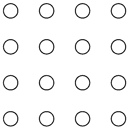
[0026] First of all, the present invention provides a method for manufacturing a semiconductor device, the manufacturing process of which is shown in the appended Figure 1-20 .

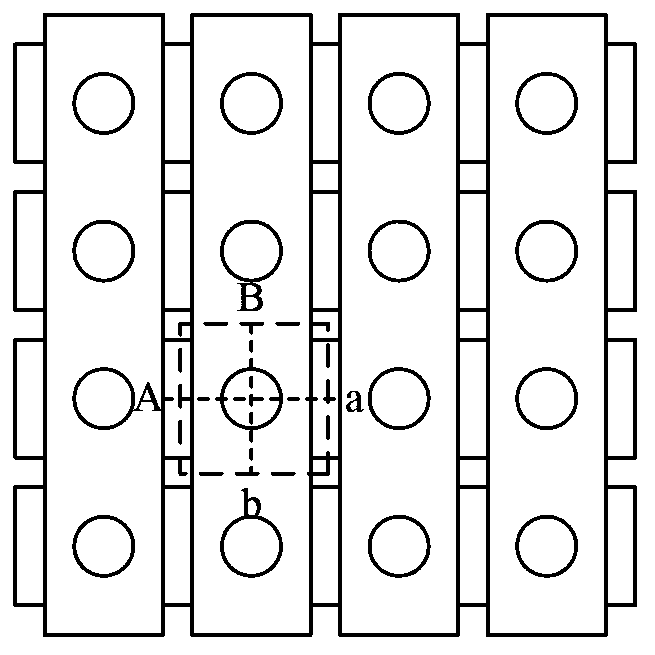
[0027] First, see attached figure 1 , is a layout of the 1T-DRAM device structure and array in the embodiment of the present invention, including three layers. figure 1 A 1T-DRAM unit is inside the dotted box. The horizontal dotted line Aa indicates the direction along which the bit line extends, and the vertical dotted line Bb indicates the direction along which the word lin...


PUM


Abstract

The present invention provides a vertical nanocolumn 1T-DRAM device and array based on SiGe energy band engineering, which adopts a vertical nanocolumn transistor, and uses epitaxy to form a stacked layer respectively as a channel region and a drain region. The design of the drain region provides a large space, which provides many implementation solutions for the improvement of 1T-DRAM performance; at the same time, the structure of the vertical transistor is conducive to the integration of the SiGe channel region, using epitaxial SiGe as the channel region, using SiGe and The difference in Si valence band creates a potential well of holes in the channel region, which can effectively increase the current difference between the read 1 state and the read 0 state of 1T-DRAM.

Description

technical field [0001] The invention relates to the field of semiconductor devices and manufacturing methods thereof, in particular to a vertical high-integration transistor structure based on SiGe energy band engineering and a manufacturing method thereof. Background technique [0002] With the continuous shrinking of the feature size of semiconductor integrated circuit devices, the size of the traditional 1T / 1C embedded DRAM unit is shrinking, and the area of ​​its capacitor is becoming more and more difficult as scaling down, and the manufacturing process is also becoming more and more difficult. Complicated, and the compatibility with the logic device process is getting worse. Therefore, capacitorless DRAM (Capacitorless DRAM) with good compatibility with logic devices will have a good development prospect in the field of high-performance embedded DRAM of VLSI. Among them, 1T-DRAM (One Transistor Dynamic Random Access Memory) utilizing floating body effect is the main i...

Claims


Application Information

Patent Timeline
Patent Type & Authority Patents(China)
IPC IPC(8): H01L21/8242H01L27/108H10B12/00
CPCH10B12/20H10B12/01
Inventor 方雯罗军赵超
Owner INST OF MICROELECTRONICS CHINESE ACAD OF SCI
Why Eureka
Eureka Blog
Learn More