Integrated passive capacitor fan-out wafer-level packaging structure and manufacturing method

A technology of wafer-level packaging and integrated passives, applied in circuits, electrical components, electrical solid-state devices, etc., can solve problems such as factors that cannot improve the quality of circuits, properties of controlled semiconductor materials, etc., to shorten the length of electrical connections and improve electrical quality , Improve the effect of quality factor Q value

Active Publication Date: 2016-08-24
NAT CENT FOR ADVANCED PACKAGING CO LTD
View PDF4 Cites 0 Cited by
  • Summary
  • Abstract
  • Description
  • Claims
  • Application Information

AI Technical Summary

Problems solved by technology

Existing integrated passive capacitors are limited by the semiconductor material properties of silicon materials, and cannot improve the quality factor of their circuits

Method used


Image

  • Integrated passive capacitor fan-out wafer-level packaging structure and manufacturing method
  • Integrated passive capacitor fan-out wafer-level packaging structure and manufacturing method
  • Integrated passive capacitor fan-out wafer-level packaging structure and manufacturing method

Examples


Embodiment Construction

[0030] The present invention will be further described below in conjunction with specific drawings.

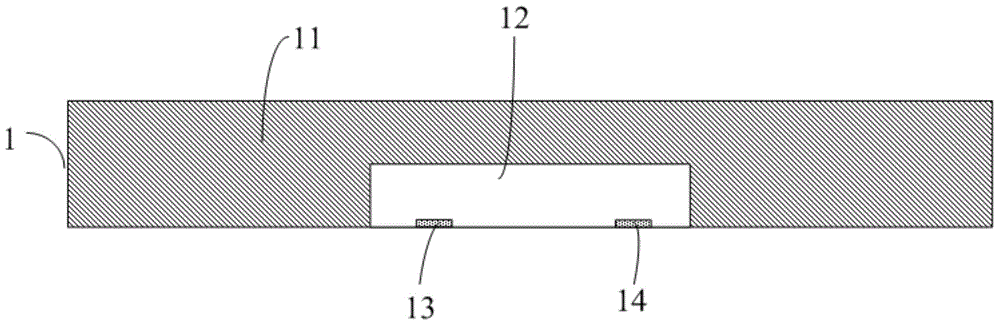
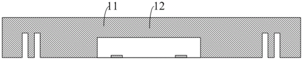
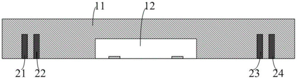
[0031] Such as Figure 10 As shown: the integrated passive capacitance fan-out wafer level packaging structure includes a fan-out package body 1, and the fan-out type package body 1 includes a plastic package body 11 and a chip 12 plastically sealed in the plastic package body 11, and the front side of the chip 12 With the first electrode 13 and the second electrode 14, the front of the chip 12 is flush with the front of the plastic package 11; two sets of capacitors are arranged in the plastic package 11, respectively the first metal post 21, the second metal post 22, The third metal post 23 and the fourth metal post 24, the first metal post 21 and the second metal post 22 are located on one side of the chip 12, and the third metal post 23 and the fourth metal post 24 are located on the other side of the chip 12; The front side of the plastic package 11 is provided with an i...


PUM


Abstract

The invention relates to an integrated passive capacitance fan-out wafer-level packaging structure and a manufacturing method, including a plastic package and a chip; the feature is that a first metal post, a second metal post, a third The first metal post and the second metal post are located on one side of the chip, and the third metal post and the fourth metal post are located on the other side of the chip; The first metal layer, the second metal layer, the third metal layer and the fourth metal layer are arranged in the layer, the first metal layer is connected with the first metal column, the second metal layer is connected with the second metal column and the first electrode, and the second metal layer is connected with the first metal column and the first electrode. The third metal layer is connected to the third metal column and the second electrode, and the fourth metal layer is connected to the fourth metal column; the metal layer under the bump is respectively arranged on the four metal layers, and the solder is respectively arranged on the outer surface of the metal layer under the point. ball. The invention realizes the integration of fan-out chip packaging and thin-film integrated passive passive devices, and improves the electrical quality.

Description

technical field [0001] The invention relates to an integrated passive capacitor fan-out wafer-level packaging structure and a manufacturing method, and belongs to the technical field of fan-out wafer-level packaging. Background technique [0002] Wafer-level fan-out chip packaging can replace the current bonded BGA (Ball Grid Array, PCB with ball grid array structure) and flip-chip BGA packaging. It is a low-cost, high-performance integrated packaging method. The signal, power and ground wiring of wafer-level fan-out chip packaging is directly realized through the wafer-level RDL (redistribution layer) process, which eliminates the need for wafer bump preparation and packaging substrates, thereby reducing packaging costs and can Provides better electrical performance than conventional wire bond BGA and flip chip BGA packages. Thin-film integrated passive technologies generally offer the best functional density, as well as the highest integration and lightest volume. Howeve...

Claims


Application Information

Patent Timeline
Patent Type & Authority Patents(China)
IPC IPC(8): H01L23/64H01L23/498H01L21/02H01L21/48
CPCH01L24/19H01L2224/12105H01L2224/19H01L2224/24195H01L2924/181H01L2924/00H01L2924/00012
Inventor 孙鹏徐健王宏杰何洪文
Owner NAT CENT FOR ADVANCED PACKAGING CO LTD
Why Eureka
Try Eureka