Nitride semiconductor structure and semiconductor light-emitting component

A nitride semiconductor and semiconductor technology, which is applied in the direction of semiconductor devices, electrical components, circuits, etc., can solve the problems of affecting the luminous efficiency of light-emitting diodes, the reduction of luminous efficiency of light-emitting diodes, and the loss of carriers at the interface, so as to increase the internal quantum efficiency. Luminous efficiency, effect of improving carrier loss

Active Publication Date: 2014-08-06
GENESIS PHOTONICS
View PDF7 Cites 2 Cited by
  • Summary
  • Abstract
  • Description
  • Claims
  • Application Information

AI Technical Summary

Problems solved by technology

[0005] The method of using p-AlGaN as the p-type carrier blocking layer can effectively confine carriers in the quantum well layer to improve the internal quantum efficiency of light-emitting diodes; however, since the multiple quantum well structure is generally based on the quantum Well layer and GaN quantum barrier layer, and in essence, the p-AlGaN p-type carrier barrier layer and GaN quantum barrier layer have a very high lattice mismatch, making the InGaN quantum well layer trap the lattice The mismatch will be severely affected by the compressive stress, which changes the energy band structure of each quantum well layer, so that the electrons and holes in the quantum well layer are spatially separated from each other, resulting in the LED's The luminous efficiency is reduced; moreover, the above-mentioned compressive stress will also deteriorate the interface characteristics between the adjacent GaN quantum barrier layer and the InGaN quantum well layer, thereby losing carriers at the interface, and also affecting the luminous efficiency of the light-emitting diode

Method used


Image

  • Nitride semiconductor structure and semiconductor light-emitting component
  • Nitride semiconductor structure and semiconductor light-emitting component

Examples


Embodiment Construction

[0045] The purpose of the present invention and its structural design and functional advantages will be described according to the following drawings and preferred embodiments, so as to have a more in-depth and specific understanding of the present invention.

[0046] First of all, in the description of the following embodiments, it should be understood that when it is indicated that a layer (or film) or a structure is disposed "on" or "under" another substrate, another layer (or film), or another structure , which can be "directly" located on other substrates, layers (or films), or another structure, or have more than one intermediate layer between them in an "indirect" manner. The location of each layer can be described with reference to the drawings.

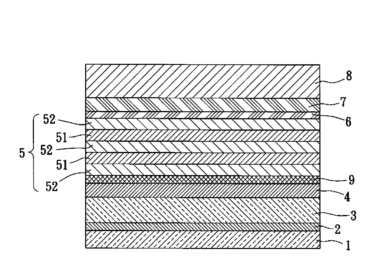
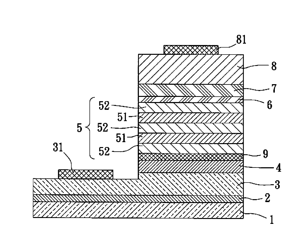
[0047] see figure 1 As shown, it is a schematic cross-sectional view of a nitride semiconductor structure provided by a preferred embodiment of the present invention. It is mainly configured with a stress control layer 6 betw...


PUM

PropertyMeasurementUnit
thicknessaaaaaaaaaa
thicknessaaaaaaaaaa

Abstract

The invention relates to a nitride semiconductor structure and a semiconductor light-emitting component. The nitride semiconductor structure is mainly characterized in that a stress control layer is arranged between a light-emitting layer and a p-type carrier barrier layer, the p-type carrier barrier layer is made of materials expressed by AlxGa1-xN, the x is larger than zero and smaller than one, the stress control layer is made of materials expressed by AlxInyGa1-x-yN, the x is larger than zero and smaller than one, the y is larger than zero and smaller than one, a sum of the x and the y is larger than zero and smaller than one, the light-emitting layer is of a multi-quantum-well structure formed by a plurality of alternated and stacked well layers and barrier layers, and one well layer is arranged between every two barrier layers. The semiconductor light-emitting component at least comprises the nitride semiconductor structure, an n-type electrode and a p-type electrode, and the n-type electrode and the p-type electrode supply power energy in a matched mode. In this way, the crystalline quality degradation problem, caused by lattice mismatching, of the p-type carrier barrier layer and the light-emitting layer can be solved through the stress control layer; meanwhile, compression stress caused by material differences and borne by the well layers can be reduced.

Description

technical field [0001] The present invention relates to a nitride semiconductor structure and a semiconductor light-emitting element, in particular to a kind of aluminum alloy arranged between the light-emitting layer and the p-type carrier blocking layer. x In y Ga 1-x-y The invention relates to a nitride semiconductor structure and a semiconductor light-emitting element of a stress control layer composed of N materials, belonging to the field of semiconductor technology. Background technique [0002] In recent years, the application of light-emitting diodes has become more and more extensive, and has become an indispensable and important component in daily life; and light-emitting diodes are expected to replace today's lighting equipment and become the solid-state lighting components of the new generation in the future. Light-emitting diodes with high efficiency and higher power will be the future trend; nitride LEDs have become one of the latest emerging optoelectronic ...

Claims


Application Information

Patent Timeline
Patent Type & Authority Applications(China)
IPC IPC(8): H01L33/12H01L33/06
CPCH01L33/06H01L33/12H01L33/32
Inventor 黄吉丰林京亮王信介吴俊德李玉柱李俊杰
Owner GENESIS PHOTONICS
Why Eureka
Try Eureka