Waveguide filter based on electromagnetically induced transparency

A technology of electromagnetic induction transparent and waveguide filter, which can be applied to waveguide devices, circuits, electrical components, etc., and can solve the problems of narrow transmission passband and increased volume.

Inactive Publication Date: 2014-08-06
UNIV OF ELECTRONIC SCI & TECH OF CHINA
View PDF5 Cites 14 Cited by
  • Summary
  • Abstract
  • Description
  • Claims
  • Application Information

AI Technical Summary

Problems solved by technology

[0003]In the design of E-plane waveguide filter, multi-level cascading is unavoidably required to increase the volume, so it is necessary to study and design a new type Waveguide filter, making it use smaller structure size to achieve better filtering performance
[0004] Th

Method used


Image

  • Waveguide filter based on electromagnetically induced transparency
  • Waveguide filter based on electromagnetically induced transparency
  • Waveguide filter based on electromagnetically induced transparency

Examples


Embodiment Construction

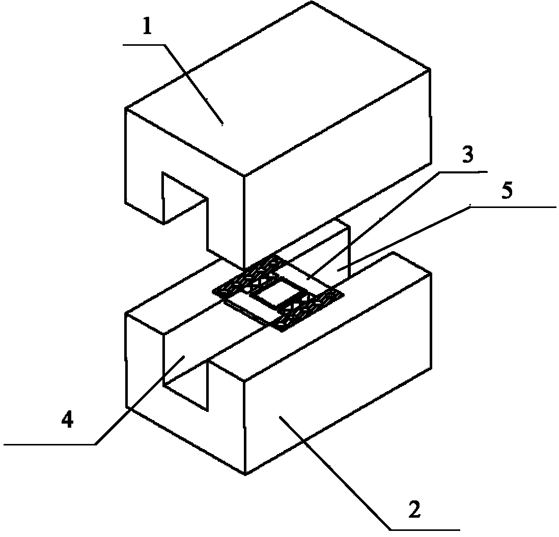
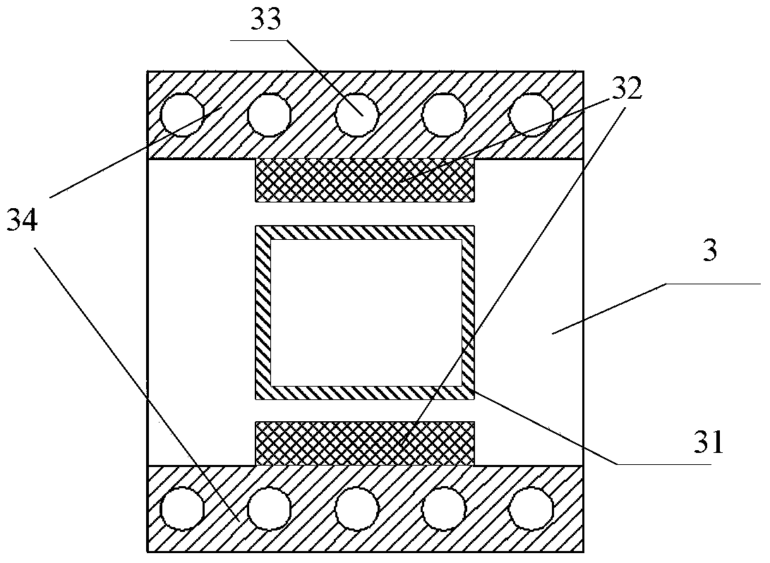
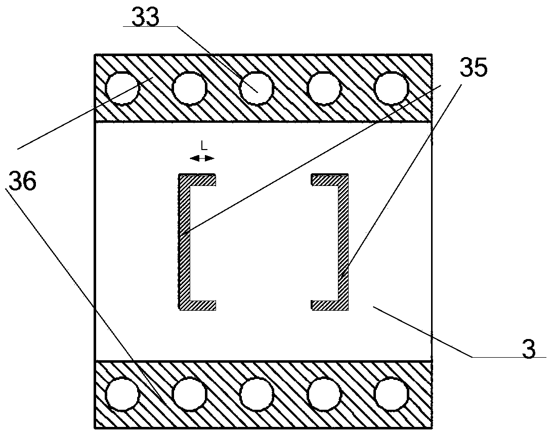
[0023] Such as figure 1 , figure 2 , image 3 As shown, a waveguide filter based on electromagnetic induction transparency includes an upper cavity 1, a lower cavity 2 constituting a standard rectangular waveguide, and a dielectric substrate 3 inserted between the upper cavity 1 and the lower cavity 2 of the standard rectangular waveguide. , a signal input port 4 and a signal output port 5; the metal microstrip structure on the front side of the dielectric substrate 3 has a rectangular metal ring 31, an out-of-band suppression sheet 32, two rows of metallized through holes 33 and a grounding extension strip 34, and the dielectric substrate 3 The metal microstrip structure on the back has two symmetrical C-shaped resonant structures 35 and a grounded epitaxial strip 36;

[0024] The rectangular metal ring 31 on the front of the dielectric substrate 3 and the two symmetrical C-shaped resonant structures 35 on the back of the dielectric substrate 3 interact to generate two pas...


PUM


Abstract

The invention discloses a waveguide filter based on electromagnetically induced transparency. The waveguide filter comprises an upper cavity, a lower cavity, a medium substrate, a signal input port and a signal output port, wherein the upper cavity and the lower cavity form a standard rectangular waveguide, and the medium substrate is inserted into the portion between the upper cavity and the lower cavity of the standard rectangular waveguide. A rectangular metal ring, an out-of-band rejection sheet, two rows of metallized through holes and a grounding epitaxial band are arranged in a metal micro-strip structure on the front face of the medium substrate, and two symmetric C-shaped resonance structures and a grounding epitaxial band are arranged on a metal micro-strip structure on the back face of the medium substrate. The rectangular metal ring located on the front side of the medium substrate and the two symmetric C-shaped resonance structures located on the back face of the medium substrate interact to generate a passing band of an electrically induced transparent window and a passing band of a magnetically induced transparent window, namely, the electromagnetically induced transparency effect is formed, upper sidebands and lower sidebands of the passing bands of the waveguide filter obtained through the effect are respectively provided with a transmission zero, high selectivity is achieved, and the waveguide filter is compact in structure and easy to design.

Description

technical field [0001] The invention relates to microwave and millimeter wave filter design technology, in particular to a new method for waveguide filter design. Background technique [0002] Waveguide filters have been widely used in many microwave and millimeter wave systems due to their small loss and large power capacity. There are various implementation techniques such as direct coupled resonators, evanescent mode waveguide filters, multimode waveguide filters, and E-plane waveguide filters. Among them, the direct coupling resonant cavity design method has flexible design, good square coefficient and low loss, but its processing is more complicated, the cost is high, and it is not easy to carry out mass production. The E-plane waveguide filter is simple to process, low in cost, suitable for mass production, and more flexible in design, but the traditional E-plane waveguide filter must be multi-staged in order to obtain excellent filter performance, which inevitably ca...

Claims


Application Information

Patent Timeline
IPC IPC(8): H01P1/207
Inventor 林先其靳俊叶于家伟江源张瑾樊勇
Owner UNIV OF ELECTRONIC SCI & TECH OF CHINA
Why Eureka
Try Eureka