Efficient photovoltaic isomerism solder strip

A photovoltaic and heterogeneous technology, applied in photovoltaic power generation, electrical components, circuits, etc., can solve the problems of reducing welding stress, welding fastness, and stress, and achieve the goal of reducing welding stress, ensuring welding strength, and optimizing guidance Effect

Active Publication Date: 2014-08-13
FUNDANT JIANGSU ADVANCED MATERIALS CO LTD
View PDF8 Cites 18 Cited by
  • Summary
  • Abstract
  • Description
  • Claims
  • Application Information

AI Technical Summary

Problems solved by technology

[0009] The technical problem to be solved by the present invention is: in order to reasonably ensure that the reflective multiplexing / stress reduction of the interconnection ribbon is realized through the surface heterogeneity of the conductive baseband of the interconnection ribbon, and to solve the problem of the difference between the heterogeneous ribbon and the battery sheet in the environment of the automatic stringer welding machine. The welding fastness between the joints is reduced / the risk of false welding is increased. The present invention provides a cost-effective high-efficiency photovoltaic system for simultaneously realizing partial reflective reuse of the surface of the welding strip, reducing welding stress, ensuring welding strength, and balancing the confluence power loss caused by slotting. Heterogeneous Ribbon

Method used


Image

  • Efficient photovoltaic isomerism solder strip
  • Efficient photovoltaic isomerism solder strip
  • Efficient photovoltaic isomerism solder strip

Examples


Embodiment 1

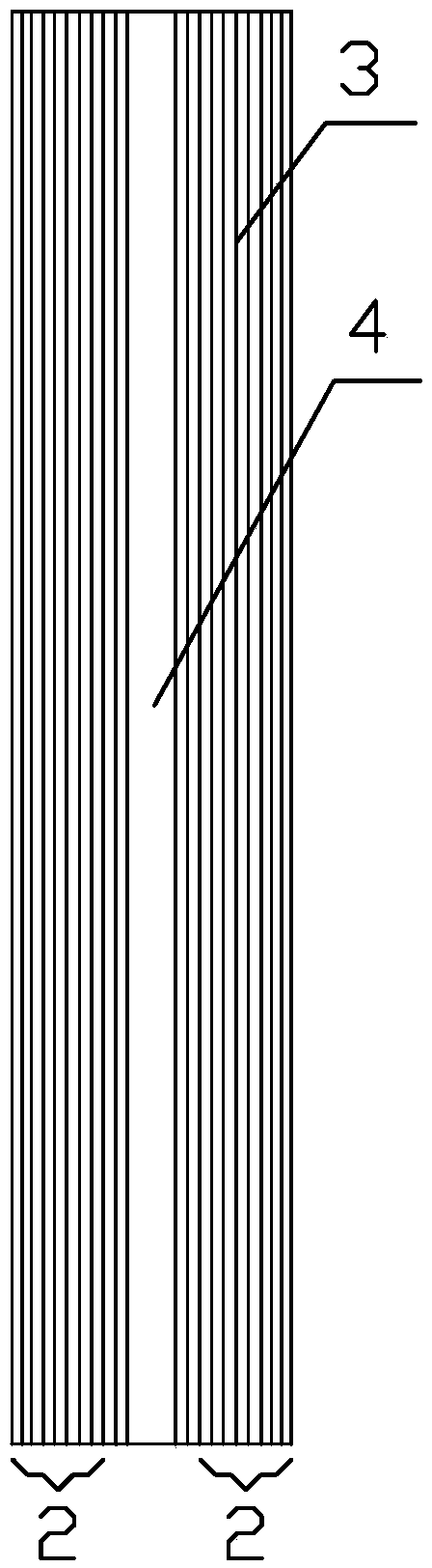
[0049] TU1 oxygen-free copper is selected as the conductive baseband 1, such as figure 1 As shown, there are two groove sets 2 along the length direction of the conductive substrate 1 on one of its wide surfaces, and the two groove sets 2 are respectively arranged on both sides of the wide surface. The V-shaped groove 3 is a linear V-shaped groove in which the intersection line of the two hypotenuses of the groove is a straight line. Of course, it can also be a curved V-shaped groove in which the intersection line of the two hypotenuses of the groove is a curve, etc. other variants.

[0050] A rectangular coupling platform 4 extending along the length direction of the conductive base strip 1 is left between the two groove sets 2. The height of the coupling platform 4 is equal to the highest point of the V-shaped groove 3. The coupling platform 4 The diameter of the largest inscribed circle of the V-shaped groove is 0.1mm; the V-shaped angle of the V-shaped groove is 138°, and...

Embodiment 2

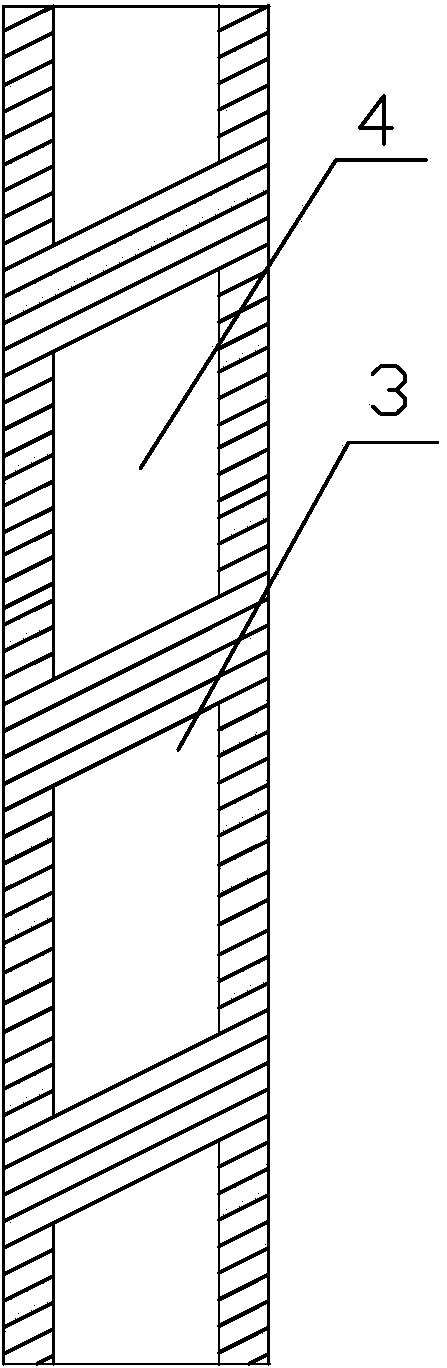
[0057] TU1 oxygen-free copper is selected as the conductive baseband 1, such as figure 2 As shown, there is a set of grooves 2 on one of its wide surfaces, each set of grooves 2 is composed of a plurality of continuous V-shaped grooves 3, and a parallelogram coupling platform 4 is left between different sets of grooves 2, the said The height of the coupling platform 4 is equal to the highest point of the V-shaped groove 3, the diameter of the largest inscribed circle of the coupling platform 4 is 0.5mm, and the maximum length along the length direction of the conductive base strip 1 is 3.0mm; the coupling platform 4 There are V-shaped grooves 3 all around; the V-shaped angle of the V-shaped groove 3 is 75°, the V-shaped groove 3 forms an angle of 30 degrees with the length direction of the conductive base strip 1, and the parallelogram has two sides and the direction of the V-shaped groove 3 Parallel; the depth h of the V-shaped groove 3 is 0.08 mm; the surface area of ​​the ...

Embodiment 3

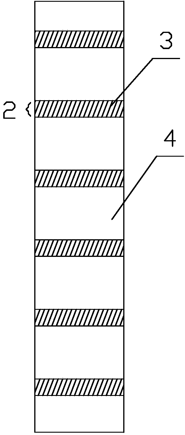
[0064] TU1 oxygen-free copper is selected as the conductive baseband 1, such as image 3 As shown, one wide surface has groove sets 2 arranged at intervals along the length direction of the wide surface, and each groove set 2 is composed of a plurality of continuous V-shaped grooves 3, and parallel gaps are left between different groove sets 2. A quadrilateral coupling platform 4, the length of the coupling platform 4 in the width direction of the wide surface is equal to the width of the wide surface, the width is 1.6 mm, and the diameter of the largest inscribed circle is 0.5 mm, which is smaller than the width of the wide surface where it is located. The maximum length along the length direction of the conductive base strip 1 is 0.5mm; the height of the coupling platform 4 is equal to the highest point of the V-shaped groove 3; the V-shaped angle of the V-shaped groove 3 is 120°, and the V-shaped groove 3 and the conductive base strip The length direction of 1 forms an angl...


PUM

PropertyMeasurementUnit
diameteraaaaaaaaaa
diameteraaaaaaaaaa
diameteraaaaaaaaaa

Abstract

The invention relates to an efficient photovoltaic isomerism solder strip. The solder strip comprises an electric conduction base strip made of metal simple substances or alloy material, and the base strip is provided with an upper wide surface and a lower wide surface. V-shaped grooves and a coupling platform are distributed on at least one wide surface of the electric conduction base strip. The depth h of the V-shaped grooves is 0.055 mm<h<0.15 mm. The diameter of the maximum inscribed circle of the coupling platform is larger than or equal to 0.10 mm. The maximum length of the platform in the length direction of the electric conduction base strip is smaller than 50 mm. The optimally designed V-shaped grooves and the coupling platform are manufactured on the surface of the electric conduction base strip, and a high-cost-performance custom design scheme is provided for partial reuse of reflected light on the surfaces of the solder strip, reduction of soldering stress, a guarantee of soldering strength and current collecting electrical loss caused by equalization grooving.

Description

technical field [0001] The invention belongs to the technical field of photovoltaic ribbon processing, and in particular relates to a high-efficiency photovoltaic heterogeneous ribbon. Background technique [0002] With the rapid development of the world economy, energy consumption is increasing, and all countries in the world need the application and popularization of new energy. As the greenhouse gas effect caused by carbon dioxide emissions causes global warming and causes natural disasters, the demand for clean and renewable energy is particularly strong in countries around the world. Since the global crisis caused by the subprime mortgage crisis in the United States in 2007 has spread and expanded, in order to stimulate economic growth, countries have adopted more active measures to encourage the use of renewable energy. The Obama administration of the United States proposed to invest 150 billion US dollars in clean energy in the next 10 years; the European Union set a...

Claims


Application Information

Patent Timeline
Patent Type & Authority Applications(China)
IPC IPC(8): H01L31/05H01L31/054
CPCY02E10/52Y02E10/50H01L31/05H01L31/02008H01L31/0508H01L31/0547
Inventor 励征
Owner FUNDANT JIANGSU ADVANCED MATERIALS CO LTD
Why Eureka
Try Eureka