Hole drilling method for printed circuit boards

A hole processing method and printed substrate technology, which are applied in the fields of printed circuit, metal processing, printed circuit manufacturing, etc., can solve the problems of deviation in plating thickness, reduced reliability of electrical connection, inability to facilitate hole processing, etc., and increase the number of processes , the effect of improving reliability

Inactive Publication Date: 2017-04-12
HITACHI SEIKO LTD
View PDF10 Cites 0 Cited by
  • Summary
  • Abstract
  • Description
  • Claims
  • Application Information

AI Technical Summary

Problems solved by technology

If the surface roughness of the inner wall of the blind hole 5 is deteriorated as described above, the thickness of the plating layer formed in the electroplating process of the conductive plating layer will vary, thereby reducing the reliability of the electrical connection between the conductor layer 1a and the conductor layer 1b. reduce
[0019] In short, in conventional laser drilling, since it is necessary to strictly control the setting value of the laser energy intensity in order to maintain the processing accuracy of the hole, there is a problem that the drilling process cannot be performed conveniently.

Method used


Image

  • Hole drilling method for printed circuit boards
  • Hole drilling method for printed circuit boards
  • Hole drilling method for printed circuit boards

Examples


Embodiment 1

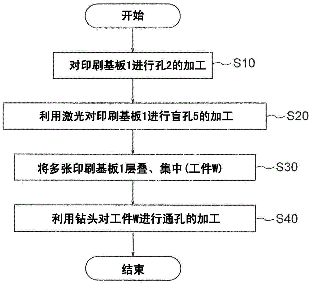
[0043] figure 1 It is a flow chart showing the overall processing procedure of the method of drilling the printed circuit board 1 according to the first embodiment of the present invention.

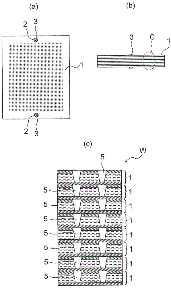
[0044] In this processing sequence, firstly, the laser pair using the laser processing machine and the Figure 7 (a)~ Figure 7 Before the printed circuit board 1 having the same printed circuit board structure as described in (c) is subjected to hole processing, a process of forming peripheral holes 2 for positioning and fixing by using a drill at a predetermined position on the peripheral portion of the printed circuit board 1 is performed. This is a step of processing the (peripheral) hole 2 on the printed circuit board 1 (step S10 ). In addition, this process is a preparatory process before carrying out the following 1st process.

[0045] Next, a first step of processing a hole from the conductor layer 1a to the surface of the conductor layer 1b at a predetermined position of the pr...

Deformed example 1

[0056] Figure 4 It is an enlarged cross-sectional view of a main part in the plate thickness direction showing a basic structure of a first modification example of a workpiece of a superimposed body that can be applied in the above-mentioned processing procedure.

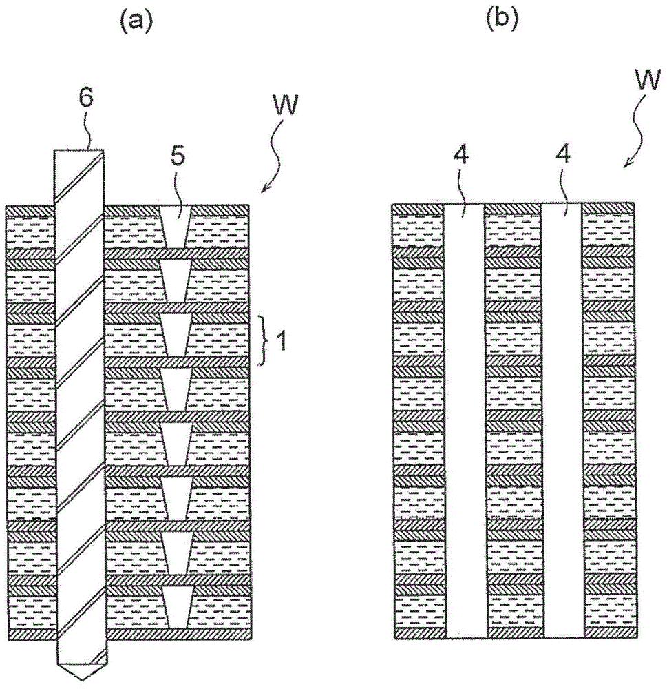
[0057] Such as Figure 4 As shown, the workpiece W1 of the superimposed body here is a printed substrate 1 that has been processed with a laser for blind holes 5 in the previous first process and a printed substrate 1 that has not been processed with blind holes 5 to carry out blind holes. 5. The processed printed circuit boards are arranged in the upper part and are sequentially stacked. Even if such a workpiece W1 is targeted, as in the case of the first embodiment, the drilling process of the through hole 4 can be performed using the drill 6 in the third step. At this time, since the processing time of the blind hole 5 in the first step can be reduced by half compared with the case where the blind hole 5 is pr...

Deformed example 2

[0059] Figure 5 It is an enlarged cross-sectional view of the main part in the plate thickness direction showing the basic structure of the second modified example of the superimposed workpiece W2 which can be applied in the above-mentioned processing procedure.

[0060] Such as Figure 5 As shown, the stacked workpiece W2 here has a laminated structure in which truncated conical through-holes 5 a are formed on each printed board 11 by laser instead of blind holes 5 formed on each printed board 1 in Example 1. That is, the through-holes 5a of the respective printed circuit boards 11 of the workpiece W2 are on the entrance side (in the Figure 5 In the example, the large diameter part) are concentrated on the upper side and the outlet side (in the Figure 5 In the example, the small diameter part) is concentrated on the lower side.

[0061] If the workpiece W2 with such a structure is used as an object, the efficiency of drilling the through hole 4 using the drill 6 in the ...


PUM


Abstract

There is provided a boring method for printed substrate capable of effectively utilizing laser and a drill to easily and effectively perform a boring process with an excellent precision without being restricted by the number of overlapped substrates. In the method, after performing a step (S10) of manufacturing peripheral holes (2) for positioning and fixing at predetermined positions of the peripheral part of the substrate (1), a step (S20) is performed by using laser on predetermined positions outside the peripheral part to manufacture via holes (5) on the substrate (1). Further, the substrates (1) manufactured with via holes are mutually overlapped to form a laminated work-piece (W), and stacking pins are inserted into the peripheral holes of the laminated work-piece W. Accordingly, after performing a step (S30) of overlapping each of the substrates (1) for compiling (the work-piece (W)), a step (S40) is performed by using a drill with a diameter (representative of the hole diameter at the inlet side of the via hole 5) larger than that of the via hole (5) to manufacture through holes in the work-piece (W).

Description

[0001] The patent application for the present invention is a divisional application of the patent application for invention with the application number 201010217581.6 and the name "Method for Perforating Printed Substrates". technical field [0002] The present invention relates to a method of drilling holes in a printed wiring board (hereinafter referred to as "printed board") for drilling holes with high precision and efficiency. Background technique [0003] Now, when electrically connecting the conductive layers arranged on the front and back sides with an insulator sandwiched between the printed board, holes for connecting to the front and back conductive layers (hereinafter referred to as connection holes) are opened in the printed board, Conductive plating is applied to the inside of the connection hole to electrically connect the positive and negative conductive layers. With recent miniaturization and high-density mounting of electronic devices, the diameter of conne...

Claims


Application Information

Patent Timeline
Patent Type & Authority Patents(China)
IPC IPC(8): H05K3/00B23B35/00B23K26/386B23K26/382B23K26/40B26F1/16
Inventor 伊藤靖道上典男河崎裕
Owner HITACHI SEIKO LTD
Why Eureka
Try Eureka