Unsealing method for flip chip device

A flip-chip and packaged device technology, applied in the field of unpacking of flip-chip devices, can solve the problems of difficult unpacking, inability to guarantee electrical characteristics, affecting related tests, etc., so as to improve the quality of unpacking, ensure completion and electrical characteristics Effect

Active Publication Date: 2014-08-27
CASIC DEFENSE TECH RES & TEST CENT
View PDF3 Cites 27 Cited by
  • Summary
  • Abstract
  • Description
  • Claims
  • Application Information

AI Technical Summary

Problems solved by technology

Due to its complex structure and the limitation of the existing unsealing method, the quality of unsealing cannot be guaranteed, which seriously affects the relevant tests after unsealing, and the electrical characteristics cannot be guaranteed
[0003] The existing unsealing method is to immerse the device in high-temperature acid to dissolve the external packaging materials (such as: molding compound, printed board, etc.), because the structure of the device using the flip-chip process is different from that of the traditional bonding process. Its unsealing difficulty is much greater than that of traditional bonding process devices, the quality after unsealing cannot be guaranteed, the damage to the silicon wafer is greater, and it is impossible to observe the interlayer structure of the printed board

Method used


Image

  • Unsealing method for flip chip device
  • Unsealing method for flip chip device

Examples


Embodiment Construction

[0039] In order to make the object, technical solution and advantages of the present invention clearer, the present invention will be described in further detail below in conjunction with specific embodiments and with reference to the accompanying drawings.

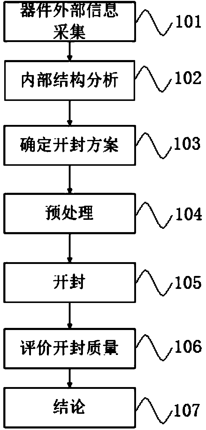
[0040] Refer to attached figure 1 , is a schematic flowchart of an embodiment of an unsealing method for a flip-chip device provided by the present invention.

[0041] The unsealing method for the flip-chip device includes:

[0042] Step 101: Collect external information of the device: use a stereo microscope to observe the device to be unsealed under a 7.1-115 times eyepiece, measure its appearance size, package thickness, and observe its package form and package material;

[0043] Step 102: Analyze the internal structure of the device: select one or more of scanning acoustic microscope, micro-focus X-ray detector, and CT detector to conduct internal structure, chip position, chip size, and internal bonding wire arrange...


PUM


Abstract

The invention discloses an unsealing method for a flip chip device. The method comprises the steps that a three-dimensional microscope is used for observing a device to be unsealed, and the appearance size, packaging thickness, packaging forms and packaging materials of the device to be unsealed are measured; one or more of a scanning acoustic microscope, a micro-focus X ray detector and a CT detector are selected to observe and record the device to be unsealed; the unsealing scheme of the device is determined according to the type of the device and the detecting results; embedding polishing or shell unsealing is used for carrying out unsealing pre-processing on the device to be unsealed; one or more of a mask etching method, a chemical etching method and a section microscopy method are used for carrying out chemical unsealing on the device to be unsealed; the interior technical parameters of the unsealed device are detected, evaluated and analyzed. Compared with a traditional unsealing method for a flip chip technology device, the unsealing method for the flip chip device has the advantages that the unsealing quality is greatly improved, and completeness and electrical characteristics of an unsealed silicon wafer are guaranteed.

Description

technical field [0001] The invention relates to the technical field of unsealing electronic devices, in particular to an unsealing method for flip-chip devices. Background technique [0002] At present, the devices that adopt the chip flip chip technology in the industry are mainly large-scale and ultra-large-scale integrated circuits in BGA packages and PGA packages. Due to its complex structure and the limitation of the existing unsealing method, the quality of unsealing cannot be guaranteed, which seriously affects the relevant tests after unsealing, and the electrical characteristics cannot be guaranteed. [0003] The existing unsealing method is to immerse the device in high-temperature acid to dissolve the external packaging materials (such as: molding compound, printed board, etc.), because the structure of the device using the flip-chip process is different from that of the traditional bonding process. The difficulty of unsealing is much greater than that of traditi...

Claims


Application Information

Patent Timeline
Patent Type & Authority Applications(China)
IPC IPC(8): H01L21/00H01L21/66
CPCH01L21/67126H01L22/12
Inventor 贺峤
Owner CASIC DEFENSE TECH RES & TEST CENT
Why Eureka
Try Eureka