
A multi-channel data cache implementation method based on fpga/cpld

An implementation method and data caching technology, which is applied in the direction of electrical digital data processing, memory systems, instruments, etc., can solve problems such as waste of storage space, complex control logic, and data packet loss, and achieve the effect of simplifying the difficulty of programming

Active Publication Date: 2017-04-26
XI AN JIAOTONG UNIV
View PDF5 Cites 0 Cited by
  • Summary
  • Abstract
  • Description
  • Claims
  • Application Information

AI Technical Summary

Problems solved by technology

Moreover, the use of EDA tools for design, synthesis, and verification can speed up the design process, reduce development risks, and shorten the development cycle. However, in the process of existing data caching, when multi-channel data is stored, the control logic of each channel data flow is relatively complicated. , it is very prone to data packet loss, and there is often a waste of storage space

Method used


Image

  • A multi-channel data cache implementation method based on fpga/cpld
  • A multi-channel data cache implementation method based on fpga/cpld
  • A multi-channel data cache implementation method based on fpga/cpld

Examples


Embodiment 1

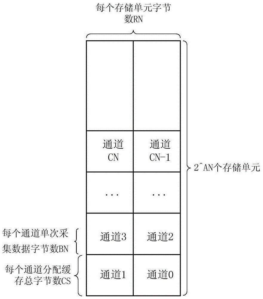
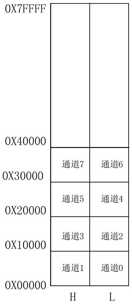
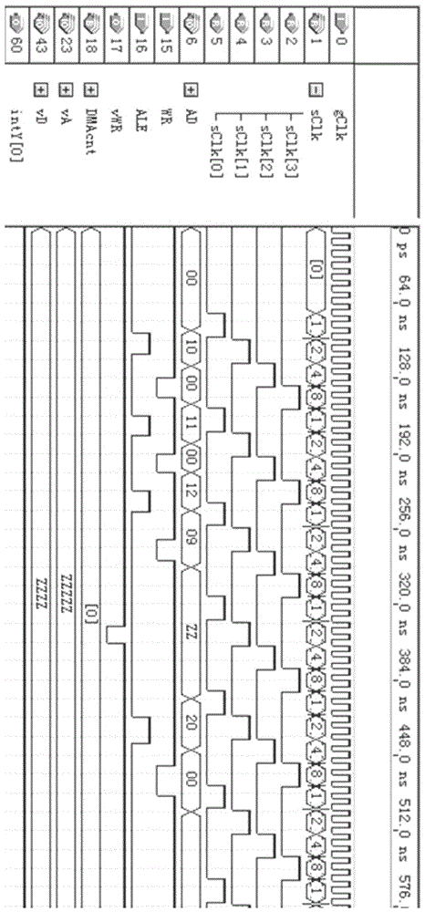
[0036] refer to figure 1 , figure 2 , image 3 , Figure 4 , Figure 5 , Image 6 , Figure 7 , Figure 8 and Figure 9 , the RAM is 512x16bit, that is, AN is equal to 19, RN is equal to 2, the number of channels is CN, etc. 8, the data collected by each channel is 32 bits, that is, BN is equal to 4, and the size of each channel in the RAM is 64K bytes. The following steps:

[0037] 1) divide the RAM, each storage unit in the RAM is 2 bytes, so each storage unit of the RAM is divided into 2 single-byte units;

[0038] 2) Divide an independent buffer area for each channel in the RAM, and the number of bytes of each buffer area is divided into 64Kbits. Among them, the buffer area occupies half of the RAM space, so the highest address of the RAM is set to 0 in the FPGA, i.e. A 18 equal to 0;

[0039] 3) The microcontroller writes the lower 8 bits of the initial target address into ADDR_BUF[7..0] of the CPLD / FPGA address register, the operation port is 0x8010, the oper...


PUM


Abstract

The invention discloses a multi-channel data cache realization method based on FPGA / CPLD, comprising the following steps: 1) dividing RAM; 2) dividing an independent buffer area for each channel in the RAM, and then encoding the channel; 3 ) Write DMA with CPLD / FPGA, specify the initial address of RAM by the single-chip microcomputer (MCU), that is, the initial address of the cache, 4) The single-chip microcomputer starts the sampling pulse, the operation port is 0x8020, latches the current data of each channel and starts the DMA, and then starts the counter DMAcnt, the counter DMAcnt is composed of two parts, the low AddrH and the high AddrL, the number of digits is equal to log2(CN / RN) plus log2(BN); 5) Driven by the DMAcnt signal, each channel samples and latches data and its own buffer area The addresses will be mapped: 6) After AddrM overflows, each channel address will be reassigned to the initial address, and this cycle can realize continuous caching. The invention can make the RAM read address and write address occupy the data line in time-sharing, and the programming of logic time sequence is simple.

Description

technical field [0001] The invention belongs to the field of electronic design automation and relates to a method for realizing multi-channel data buffering, in particular to a method for realizing multi-channel data buffering based on FPGA / CPLD. Background technique [0002] Today, when computers are widely used, the importance of data acquisition is very significant. It is a bridge connecting computers with the external physical world. It is widely used in industrial fields, automobile industry, transportation, aerospace, electric energy and civil engineering and other fields . Data buffering is an important link in the data acquisition process, especially in the field of high-speed acquisition. The data buffering technology directly limits the upper limit of the sampling frequency and affects the sampling quality. [0003] In terms of high-speed data cache, Field Programmable Gate Array (FPGA) has the incomparable advantages of ordinary microcontrollers and digital signa...

Claims


Application Information

Patent Timeline
IPC IPC(8): G06F12/0844G06F13/12
Inventor 陶涛刘毅梅雪松张东升孙挪刚姜歌东
Owner XI AN JIAOTONG UNIV
Learn More