Memory chip for imaging equipment
A storage chip and imaging equipment technology, which is applied in the fields of electrical recording process equipment using charge graphics, electrical recording technology using charge graphics, and electrical recording technology. Data security adverse effects and other issues to achieve the effect of improving reliability and practicability, simplifying the judgment process, and improving accuracy
- Summary
- Abstract
- Description
- Claims
- Application Information
AI Technical Summary
Problems solved by technology
Method used
Image

Examples
Embodiment 1
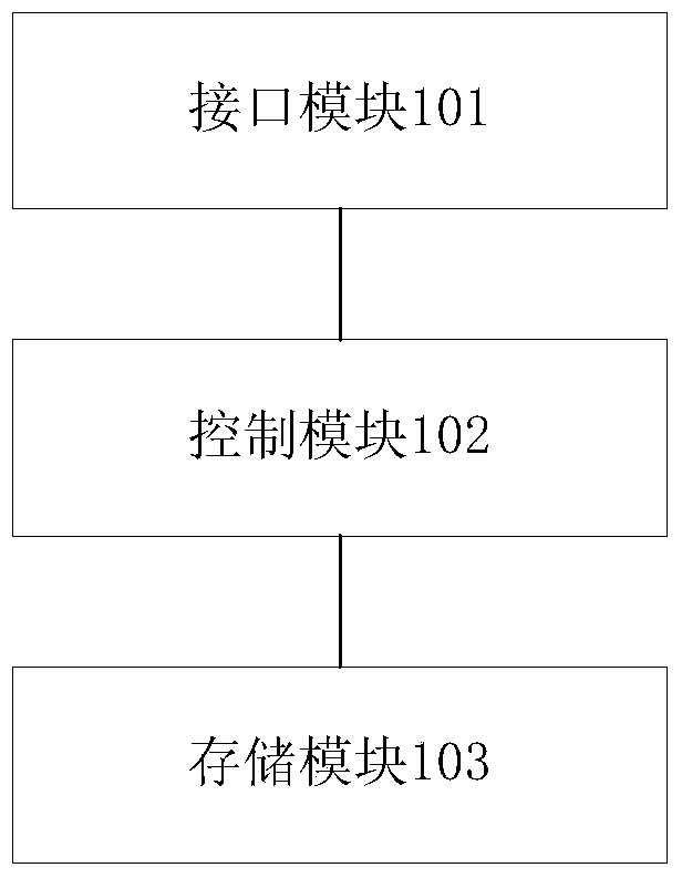
[0041] According to the use characteristics of the chip, the memory chip used in the imaging device can generally be divided into two regions, a rewritable region and a non-rewritable region. Among them, the data stored in the rewritable area is called variable data (such as the usage or remaining amount of the imaging material, etc.), and the data stored in the non-rewritable area is called immutable data (such as the imaging box model, the color of the imaging material in the imaging box, etc.) Wait).
[0042] The memory chip used in the imaging device needs to initialize the data in the chip before leaving the factory. The initialization of the memory chip is usually to use the burning equipment in the factory to write the initial data to the memory chip in batches and efficiently. This also requires that the burning device can change all the data in the memory chip, that is, the burning device can change both the variable data in the memory chip and the immutable data in ...
Embodiment 2
[0088] The type of the external controller connected to the memory chip is very important to the configuration of the data communication mode of the memory chip. This embodiment provides a memory chip for an imaging device that uses a port to determine the type of the external controller.
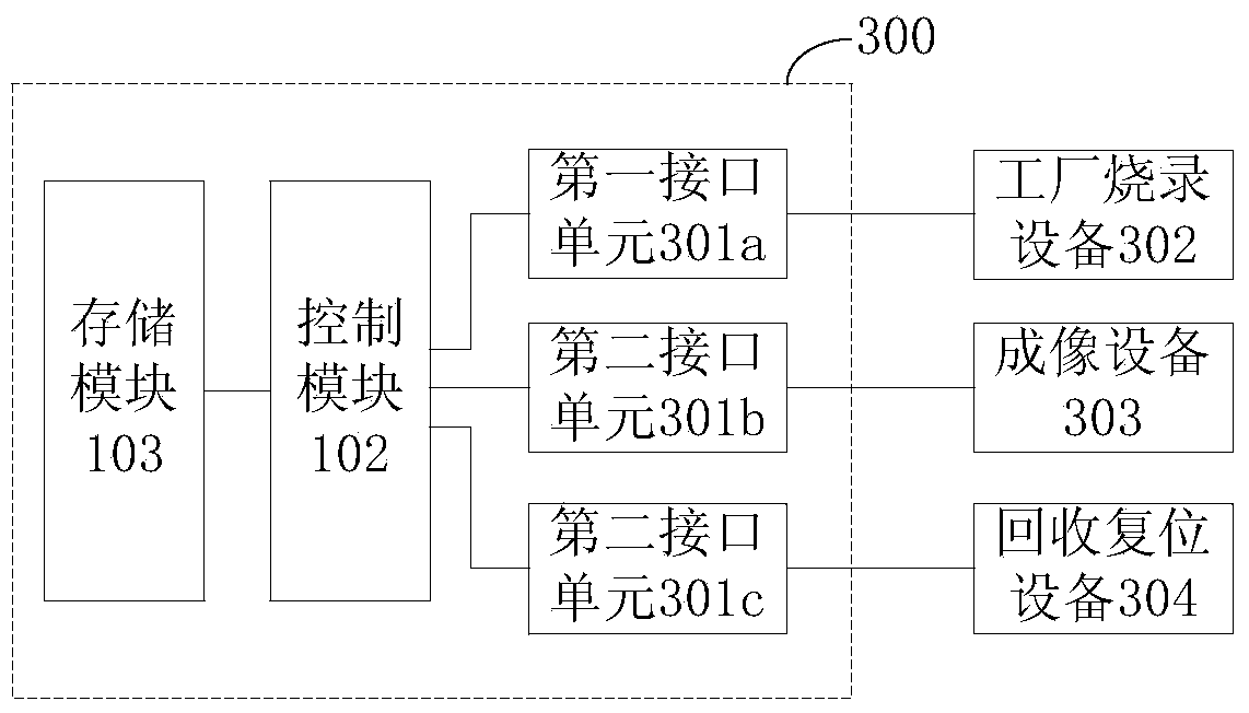
[0089] image 3 A schematic structural diagram of the memory chip provided by this embodiment is shown.
[0090] Such as image 3 As shown, the memory chip 300 provided in this embodiment includes a control module 102, a memory module 103, a first interface unit 301a, a second interface unit 301b, and a third interface unit 301c. Wherein, the first interface unit 301a, the second interface unit 301b and the third interface unit 301c are respectively connected with the factory programming device 302, the imaging device 303 and the recycling reset device 304. At the same time, the above three interface units are also connected to the control module 102 so as to transmit received signals to ...
Embodiment 3
[0097] Figure 4 A schematic structural diagram of another memory chip provided by this embodiment is shown. In addition to the interface module 101 , the control module 102 and the storage module 103 , the memory chip 300 is additionally provided with a first auxiliary interface 101 a and a second auxiliary interface 101 b. Wherein, the interface module 101 can be connected with the factory burning device 302 , the imaging device 303 or the recycling reset device 304 . When the factory programming device 302 is connected to the interface module 101, the factory programming device 302 is also connected to the first auxiliary interface 101a. When the recovery reset device 304 is connected to the interface module 101, the recovery reset device 304 is also connected to the second auxiliary interface 101b.
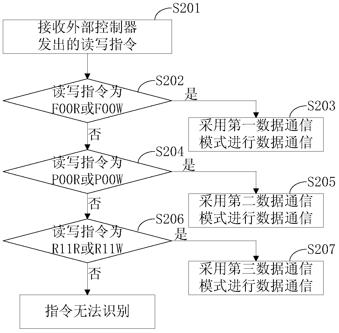
[0098] When the factory programming device 302 or the recovery reset device 304 reads and writes data to the memory chip 300 , it will send a mode start signal to the memory...
PUM
 Abstract
Description
Claims
Application Information
 - R&D
- Intellectual Property
- Life Sciences
- Materials
- Tech Scout
- Unparalleled Data Quality
- Higher Quality Content
- 60% Fewer Hallucinations
Browse by: Latest US Patents, China's latest patents, Technical Efficacy Thesaurus, Application Domain, Technology Topic, Popular Technical Reports.
© 2025 PatSnap. All rights reserved.Legal|Privacy policy|Modern Slavery Act Transparency Statement|Sitemap|About US| Contact US: help@patsnap.com