TFT (thin film transistor) backboard manufacturing method and TFT backboard structure

一种制造方法、背板的技术,应用在半导体/固态器件制造、半导体器件、电气元件等方向,能够解决接触阻抗占用部分像素面积等问题,达到提升产品良率、制程简单、效率提高的效果

Inactive Publication Date: 2014-09-10
TCL CHINA STAR OPTOELECTRONICS TECH CO LTD
View PDF9 Cites 12 Cited by
  • Summary
  • Abstract
  • Description
  • Claims
  • Application Information

AI Technical Summary

Problems solved by technology

[0009] Another object of the present invention is to provide a TFT backplane structure, which can solve the problem of contact resistance caused by pixel electrodes overlapping the source / drain and occupying part of the pixel area, so that the efficiency of AM-OLED is improved and the aperture ratio is increased. , and the manufacturing process of the TFT backplane structure is simple, and the production efficiency is high

Method used


Image

  • TFT (thin film transistor) backboard manufacturing method and TFT backboard structure
  • TFT (thin film transistor) backboard manufacturing method and TFT backboard structure
  • TFT (thin film transistor) backboard manufacturing method and TFT backboard structure

Examples


Embodiment Construction

[0041] In order to further illustrate the technical means adopted by the present invention and its effects, the following describes in detail in conjunction with preferred embodiments of the present invention and accompanying drawings.

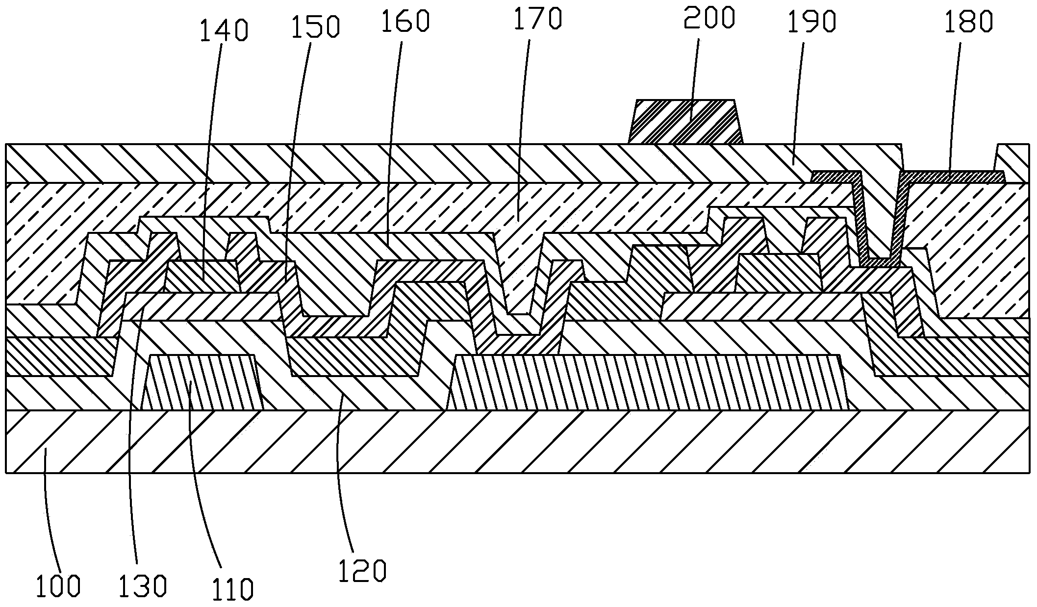
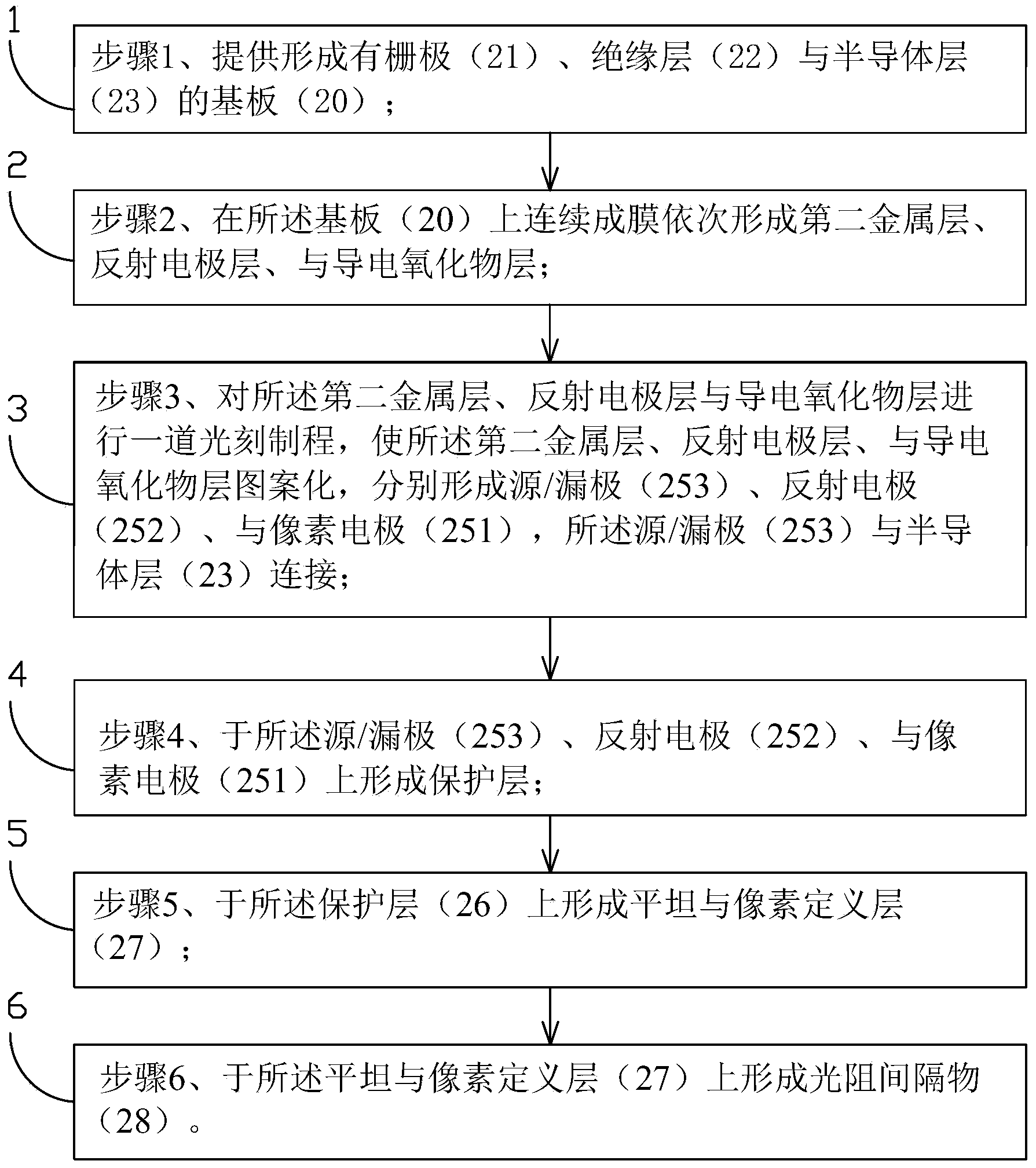
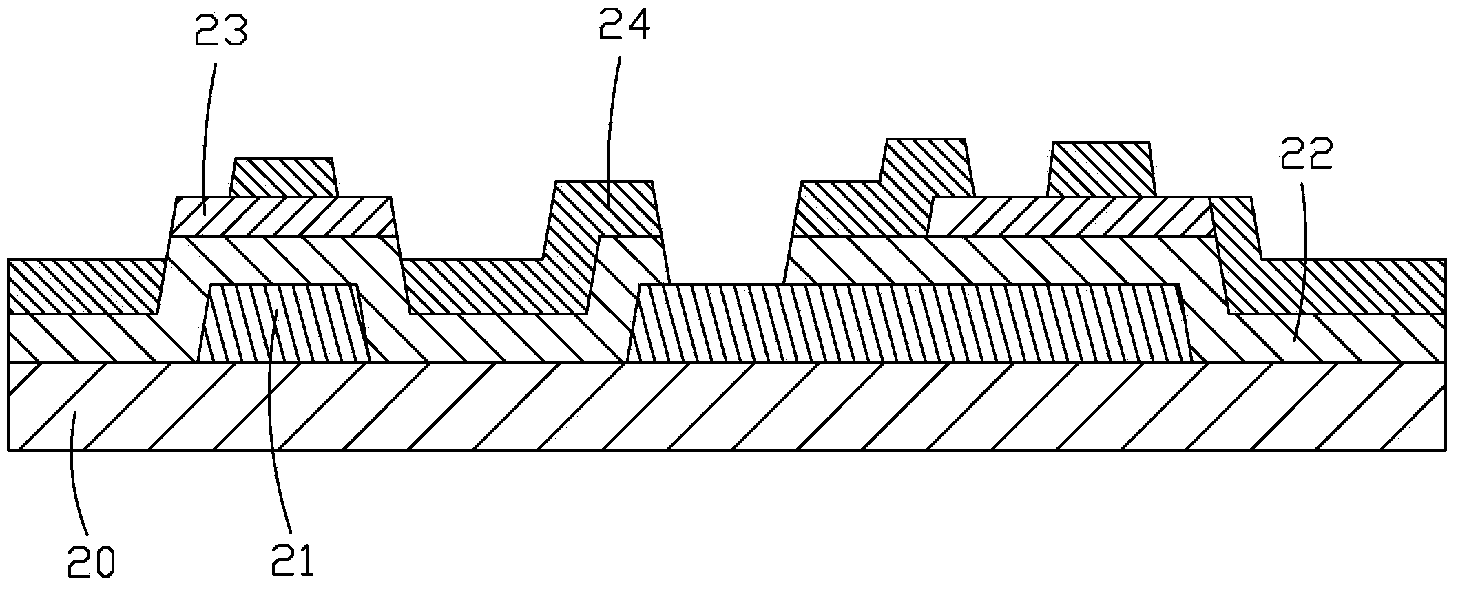
[0042] see figure 2 The flow chart of the manufacturing method of TFT backplane of the present invention, refer to simultaneously Figure 3 to Figure 7 A schematic diagram of the first embodiment of the manufacturing method of the TFT backplane of the present invention, the first embodiment is suitable for manufacturing a bottom-gate TFT backplane with an etching stopper layer. The manufacturing method of TFT backboard of the present invention comprises the following steps:

[0043] Step 1, providing a substrate 20 formed with a gate 21 , an insulating layer 22 and a semiconductor layer 23 .

[0044] The step 1 can be realized by existing technology. In step 1 of the first embodiment, the substrate 20 is a transparent substrate, preferably...


PUM


Abstract

The invention provides a TFT (thin film transistor) backboard manufacturing method and a TFT backboard structure. The TFT backboard manufacturing method includes steps of 1, providing a substrate (20) with a grid electrode (21), an insulation layer (22) and a semiconductor layer (23); 2, continuously filming to sequentially form a second metal layer, a reflecting electrode layer and a conductive oxide layer on the substrate (20); 3, subjecting the second metal layer, the reflecting electrode layer and the conductive oxide layer to photoetching processing so as to pattern the same, respectively forming source / drain electrodes (253), reflecting electrodes (252) and pixel electrodes (251) and connecting the source / drain electrodes (253) with the semiconductor layer (23); 4, forming a protecting layer on the source / drain electrode (253), the reflecting electrodes (252) and the pixel electrodes (251); 5, forming a flat pixel definition layer (27) on the protecting layer (26); 6, forming a photoresistance spacer (28) on the flat pixel definition layer (27).

Description

technical field [0001] The invention relates to the technical field of plane display, in particular to a method for manufacturing a TFT backplane and a TFT backplane structure. Background technique [0002] Flat-panel display devices have many advantages such as thin body, power saving, and no radiation, and have been widely used. Existing flat panel display devices mainly include liquid crystal display devices (Liquid Crystal Display, LCD) and organic electroluminescent display devices (Organic Light Emitting Display, OLED). [0003] Organic electroluminescent display devices have the advantages of self-illumination, no need for backlight, high contrast, thin thickness, wide viewing angle, fast response, flexible panels, wide operating temperature range, simple structure and manufacturing process, etc. characteristics, is considered to be the next generation of flat-panel display emerging application technology. [0004] OLED generally includes: a substrate, an ITO (indiu...

Claims


Application Information

Patent Timeline
Patent Type & Authority Applications(China)
IPC IPC(8): H01L21/77H01L27/12
CPCH01L27/124H01L27/1288H01L27/1225H10K59/1201H10K59/1213H10K71/00H10K71/621H10K50/81H01L21/77H01L27/12H01L27/1214
Inventor 李文辉张合静石龙强
Owner TCL CHINA STAR OPTOELECTRONICS TECH CO LTD
Why Eureka
Try Eureka