Universal easily-installed photovoltaic component and photovoltaic mounting structure using the same
A photovoltaic component and easy-to-install technology, which is applied to the support structure of photovoltaic modules, photovoltaic power generation, photovoltaic modules, etc., can solve the problems of cumbersome installation, occupation of support structure, high cost, etc., and achieve the effect of saving installation time and cost
- Summary
- Abstract
- Description
- Claims
- Application Information
AI Technical Summary
Problems solved by technology
Method used
Image

Examples
Embodiment 1
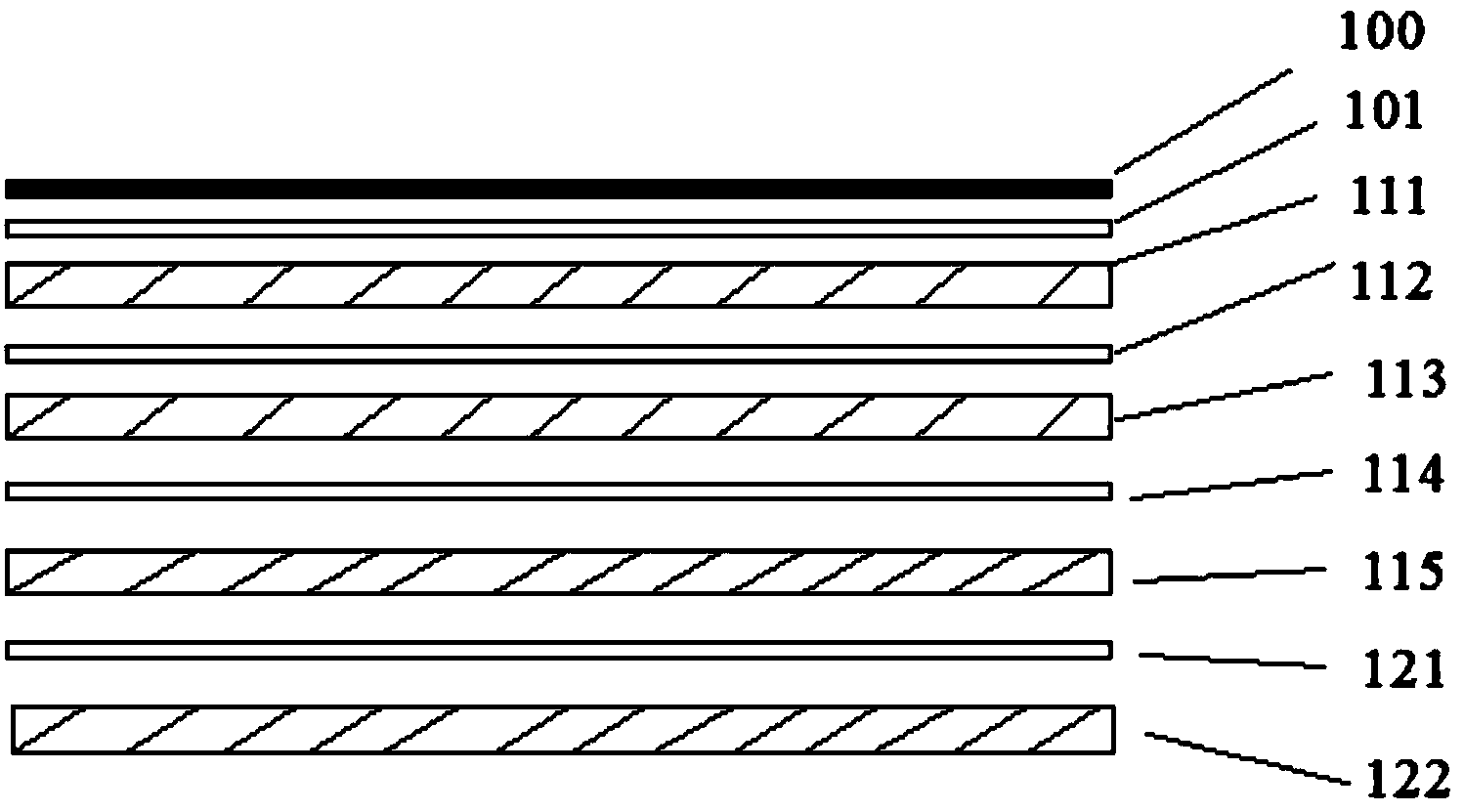
[0040] A general-purpose easy-to-install photovoltaic component, from top to bottom:
[0041] Release layer 100: PET film with a thickness of about 0.01-0.05mm;
[0042] OCA optical adhesive bonding layer 101: use 3M thin OCA tape or glue layer, the thickness is 0.025 ~ 0.10mm;
[0043] Light-receiving surface encapsulation layer 111: 0.2mm thick ETFE film is used, which has good light transmission and protection performance;
[0044] The first adhesive layer 112: using 0.5mm EVA film layer;
[0045] Photovoltaic cell layer 113: Small pieces of high-efficiency crystalline silicon cells are used, and different cells are connected by multiple copper wires;
[0046] The second adhesive layer 114: the same as the first adhesive layer 112, adopting a 0.5mm EVA film layer;
[0047] Back protective layer 115: adopt 0.2mm transparent fluorinated PET film;
[0048] The third adhesive layer 121: using 0.2mm transparent EVA;
[0049] Back support layer 122: adopt 1mm transparent hig...
Embodiment 2
[0052] A general-purpose easy-to-install photovoltaic component, from top to bottom:
[0053] Release layer 100: PET film with a thickness of about 0.01-0.05mm;
[0054] OCA optical adhesive bonding layer 101: use 3M thin OCA tape or glue layer, the thickness is 0.025 ~ 0.10mm;
[0055] Light-receiving surface encapsulation layer 111: PET film with a thickness of 0.2mm is used, which has good light transmission and protection performance;
[0056] The first adhesive layer 112: using 0.5mm EVA film layer;
[0057] Light-receiving surface packaging layer 111: use small pieces of high-efficiency crystalline silicon cells, and connect different cells through multiple copper wires;
[0058] The second adhesive layer 114: the same as the first adhesive layer 112, adopting a 0.5mm EVA film layer;
[0059] Back layer: 1mm transparent fluorinated high temperature resistant PC (polycarbonate) sunlight board, such as a thin board made of fluorinated APEC1603 material from Bayer, Germa...
PUM
| Property | Measurement | Unit |
|---|---|---|
| Thickness | aaaaa | aaaaa |
| Thickness | aaaaa | aaaaa |
| Thickness | aaaaa | aaaaa |
Abstract
Description
Claims
Application Information
 - Generate Ideas
- Intellectual Property
- Life Sciences
- Materials
- Tech Scout
- Unparalleled Data Quality
- Higher Quality Content
- 60% Fewer Hallucinations
Browse by: Latest US Patents, China's latest patents, Technical Efficacy Thesaurus, Application Domain, Technology Topic, Popular Technical Reports.
© 2025 PatSnap. All rights reserved.Legal|Privacy policy|Modern Slavery Act Transparency Statement|Sitemap|About US| Contact US: help@patsnap.com