
Layout verification method used for polysilicon cell edge structure in FinFET standard cells

A standard cell, polysilicon technology for special data processing applications, instrumentation, total factory control, etc.

Active Publication Date: 2014-09-17
TAIWAN SEMICON MFG CO LTD
View PDF5 Cites 18 Cited by
  • Summary
  • Abstract
  • Description
  • Claims
  • Application Information

AI Technical Summary

Problems solved by technology

However, the use of finFET transistors in the standard cell approach creates additional problems in verification

Method used

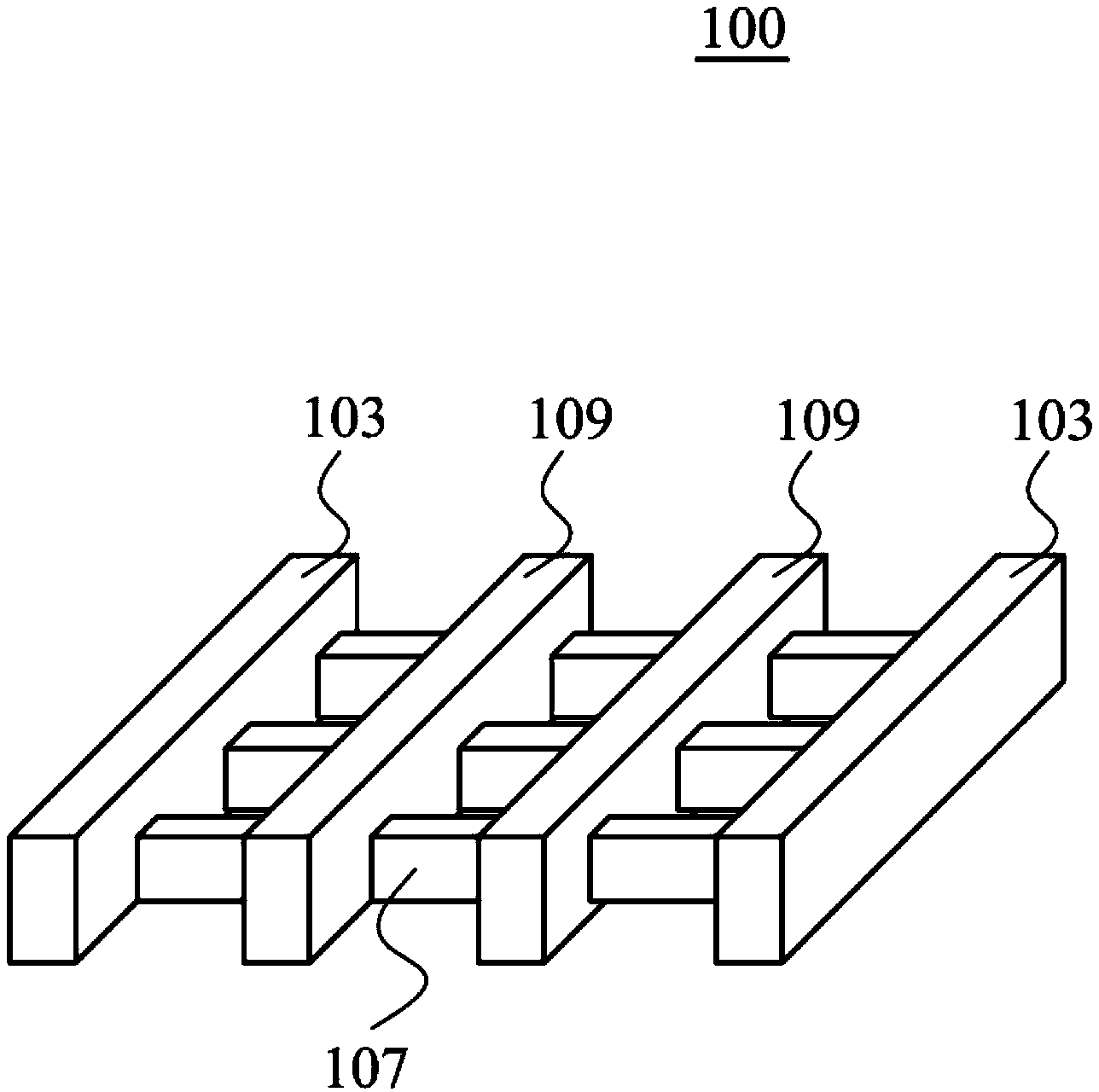
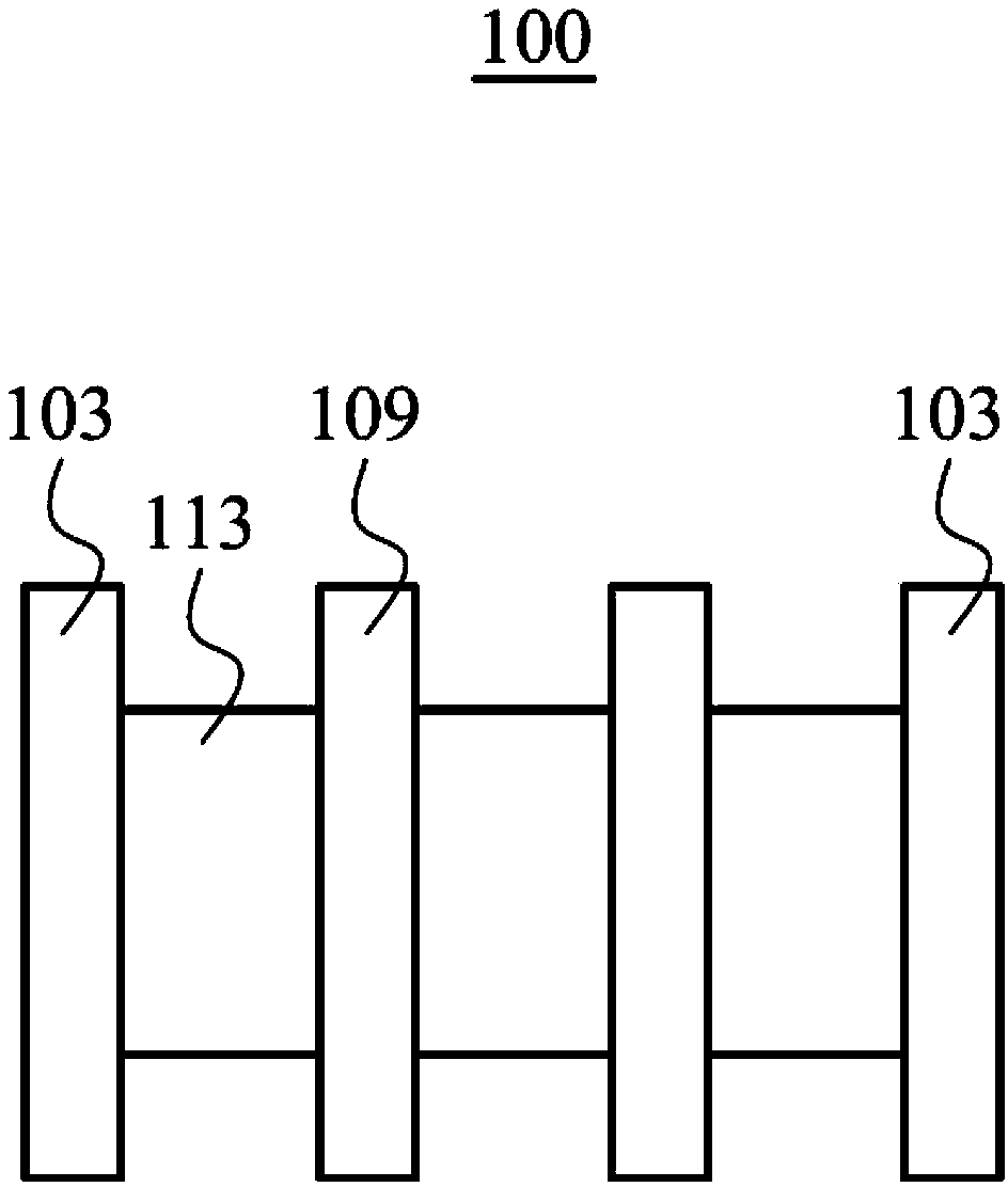
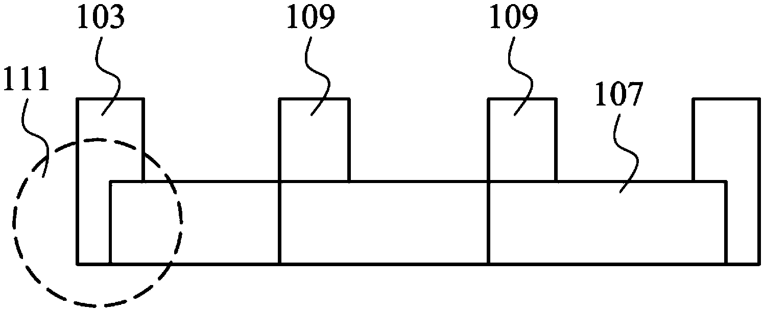

Image

  • Layout verification method used for polysilicon cell edge structure in FinFET standard cells
  • Layout verification method used for polysilicon cell edge structure in FinFET standard cells
  • Layout verification method used for polysilicon cell edge structure in FinFET standard cells

Examples


Embodiment Construction

[0060] The making and using of exemplary embodiments of the invention are discussed in detail below. It should be appreciated, however, that the described embodiments provide many applicable concepts that can be implemented in a wide variety of specific contexts. The specific embodiments discussed are merely illustrative of specific ways to make and use various embodiments, and do not limit the scope of the description or the appended claims.

[0061] In standard cell design, a user such as an integrated circuit designer uses a suite of software tools that are applied in conjunction to form a design flow. Workstations or personal computers, which can include portable and removable devices such as laptops and tablets and even smartphone devices, can be used to work with the design tools. Shared data files for the design can be stored in non-volatile memory such as a disk or flash memory device, or on a server connected to a network or even accessed on an Internet port. These ...


PUM


Abstract

The invention discloses a method for standard cells using an FinFET standard cell structure with polysilicon on OD edges. FinFET transistors are used to define the standard cells, and the standard cells comprise grid structures forming a transistor at a crossing point with a semiconductor fin. Polysilicon pseudo-structures are formed in active areas of the standard cells or edges of OD areas. In a design process, a pre-layout netlist schematic diagram for the standard cells includes a three-terminal MOS device corresponding to the polysilicon pseudo-structure at the edges of the standard cells. After automatic placement and routing processing, standard cells are employed to form a device layout, and a post-layout netlist is extracted. If two standard cells are contiguous, a single polysilicon pseudo-structure at the common boundary is formed. A layout-versus-schematic comparison is then performed in which the pre-layout netlist and the post-layout netlist are compared in order to verify the obtained layout. The invention also discloses a layout verification method used for a polysilicon cell edge structure in FinFET standard cells.

Description

[0001] This application claims the benefit of U.S. Provisional Application No. 61 / 778,036, filed March 12, 2013, entitled "Methods for Layout Verification for Polysilicon Cell Edge Structures in FinFET Standard Cell," which is incorporated by reference in its entirety incorporated into this article. [0002] Cross References to Related Applications [0003] This application is related to concurrently filed co-pending U.S. Patent Application No. TBD, entitled "Methods for Layout Verification for Polysilicon Cell Edge Structures in FinFET Standard Cells using Filter," Attorney Docket No. TSM12-1366, This application is incorporated herein by reference in its entirety. technical field [0004] Embodiments of the invention generally relate to the use of FinFET transistors to form standard cells for integrated circuits, and more particularly, to the use of standard cell methodologies in the manufacture of integrated circuits using automated place and route and design tools. Metho...

Claims


Application Information

Patent Timeline
Patent Type & Authority Applications(China)
IPC IPC(8): G06F17/50
CPCG06F17/50G06F30/398G06F2119/18Y02P90/02
Inventor 陈仕昕刘凯明
Owner TAIWAN SEMICON MFG CO LTD
Learn More