Semiconductor packaging structure

A packaging structure and semiconductor technology, which is applied in the direction of semiconductor devices, semiconductor/solid-state device parts, electric solid-state devices, etc., can solve the problems of increasing or unfavorable packaging structure integration, large volume, etc., to achieve increased integration and reduced area , small size effect

Inactive Publication Date: 2014-09-24
NANTONG FUJITSU MICROELECTRONICS
View PDF9 Cites 7 Cited by
  • Summary
  • Abstract
  • Description
  • Claims
  • Application Information

AI Technical Summary

Problems solved by technology

[0005] The existing packaging structure occupies a large volume, which is no

Method used


Image

  • Semiconductor packaging structure
  • Semiconductor packaging structure
  • Semiconductor packaging structure

Examples


Embodiment Construction

[0012] The specific embodiments of the present invention will be described in detail below in conjunction with the accompanying drawings.

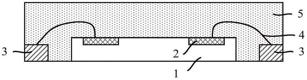
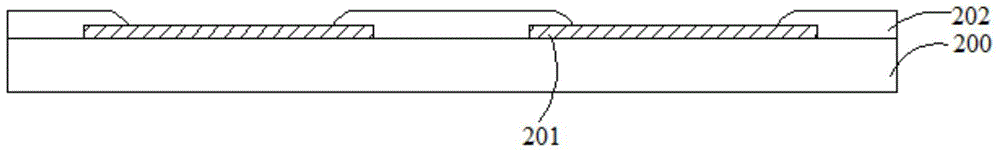
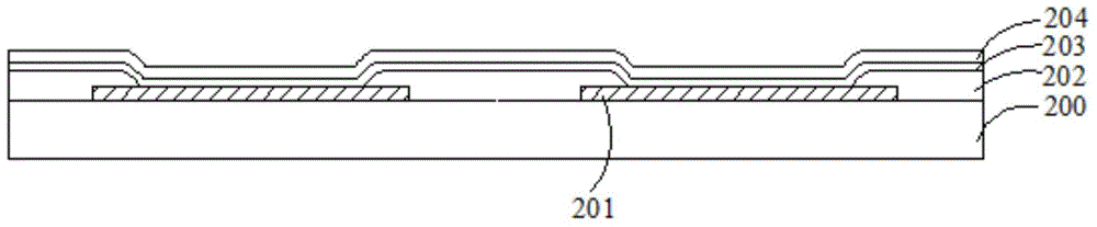
[0013] First, refer to figure 2 , provide a semiconductor chip 200, the surface of the semiconductor chip 200 is provided with a bonding pad 201 and a passivation layer 202, and the passivation layer 202 is provided with a first opening exposing the bonding pad 201.

[0014] The pad 201 is the functional output terminal of the chip 200, and finally realizes the conductive transition of the electrical function through the post-formed stud bump 206; the material of the passivation layer 202 includes silicon oxide, silicon nitride, silicon oxynitride, poly Dielectric materials such as imide and benzenetributene or their mixtures are used to protect the circuits in the chip 200 .

[0015] It should be noted that the pad and passivation layer of the chip can be the initial pad and the initial passivation layer of the chip, and can also be a t...


PUM

PropertyMeasurementUnit
Thicknessaaaaaaaaaa
Thicknessaaaaaaaaaa
Thicknessaaaaaaaaaa

Abstract

The invention provides a semiconductor packaging structure. The semiconductor packaging structure comprises a chip. The surface of the chip is provided with a pad and a passivation layer. The passivation layer is provided with a first opening which exposes the pad. The pad is provided with a seed layer and columnar bumps. The seed layer is connected with the pad. The columnar bumps are stacked on the seed layer. The semiconductor packaging structure also comprises a lead frame which is provided with a plurality of discrete pins, and an inner pin and an outer pin are arranged at two opposite faces of each pin. The chip is installed on the lead frame in an inverted way. The columnar bumps are connected with the inner pin. The semiconductor packaging structure also comprises a plastic package layer, the chip, the columnar bumps and the lead frame are sealed by the plastic package layer and the outer pin is exposed. According to the semiconductor packaging structure, the occupied lateral area of the packaging structure is reduced, the volume of the whole packaging structure is reduced, and the integration of the packaging structure is raised.

Description

[0001] This application is a divisional application of the Chinese invention patent application filed on February 24, 2014 with the application number 201410061904.5 and the title of the invention is "semiconductor packaging structure". technical field [0002] The invention relates to the field of semiconductor packaging, in particular to a semiconductor packaging structure. Background technique [0003] With the development of electronic products such as mobile phones and notebook computers towards miniaturization, portable, ultra-thin, multimedia and low-cost to meet the needs of the public, high-density, high-performance, high-reliability and low-cost packaging forms and their Assembly technology has developed rapidly. Compared with expensive BGA (Ball Grid Array) and other packaging forms, new packaging technologies that have developed rapidly in recent years, such as Quad Flat No-lead QFN (Quad Flat No-leadPackage) packaging, due to their good thermal performance and e...

Claims


Application Information

Patent Timeline
IPC IPC(8): H01L23/498
CPCH01L2224/16245
Inventor 夏鑫丁万春高国华
Owner NANTONG FUJITSU MICROELECTRONICS
Why Eureka
Try Eureka