Reconstruction wafer structure with bared chip back and manufacturing method thereof
What is AI technical title?
AI technical title is built by PatSnap AI team. It summarizes the technical point description of the patent document.
A chip and backside technology, which is applied to the reconstructed wafer structure and manufacturing field exposed on the backside of the chip, can solve the problems of high cost and low cost, and achieve the effects of low cost, easy heat dissipation, and process saving
Active Publication Date: 2014-09-24
NAT CENT FOR ADVANCED PACKAGING
View PDF4 Cites 3 Cited by
Summary
Abstract
Description
Claims
Application Information
AI Technical Summary
This helps you quickly interpret patents by identifying the three key elements:
Problems solved by technology
Method used
Benefits of technology
Problems solved by technology
[0006] The embodiment of the present invention provides a reconstructed wafer structure and manufacturing method with exposed chip backside, which is used to solve the technical problem of high cost caused by the need to use high-precision and high-cost plastic packaging molds in the prior art, and has the advantage of eliminating the need to use high-precision molds , low-cost technical effect
Method used
Image
Click on the blue label to locate the original text in one second.
Reading with bidirectional positioning of images and text.
Examples
Embodiment 1
[0031] In order to enable those skilled in the art to understand the present invention in more detail, the present invention will be described in detail below in conjunction with the accompanying drawings.
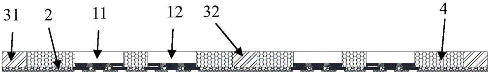
[0032] Such as figure 1 said, figure 1 It is a reconstituted wafer structure with an exposed chip backside in an embodiment of the present invention, wherein the structure includes:
[0033] the first chip 11;
[0034] second chip 12;
[0035] Rewiring layer 2, the first chip 11 and the second chip 12 are disposed on the rewiring layer 2, wherein the first chip 11 and the second chip 12 are a distance from the rewiring layer 2 by a distance of distance a;
[0036] The first height-limiting block 31 and the second height-limiting block 32, the first height-limiting block 31 and the second height-limiting block 32 are arranged on the rewiring layer 2, wherein the first height-limiting block 31 There is a second distance b between the second height limiting block 31 and ...
Embodiment 2
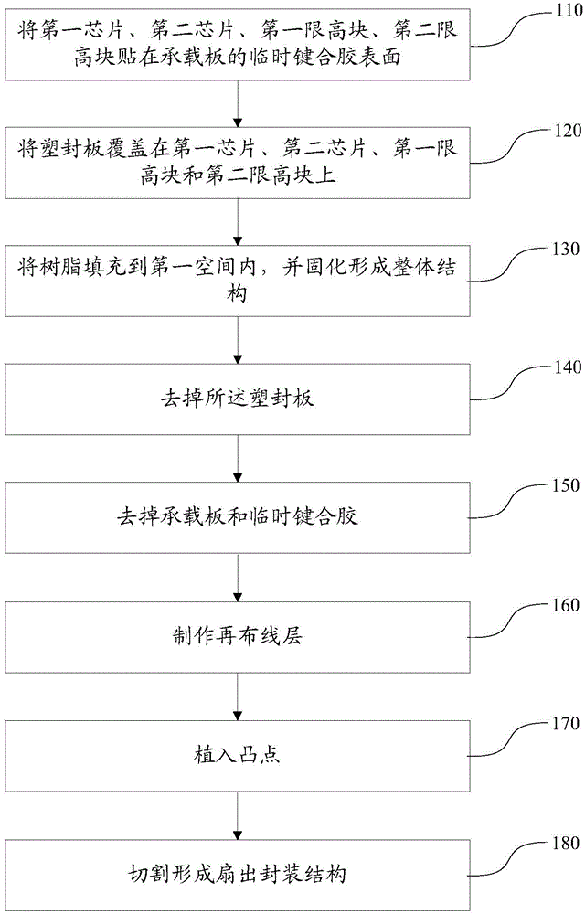
[0046] Such as Figure 2-10 As shown, the embodiment of the present invention also provides a method for fabricating a reconstructed wafer structure with an exposed chip backside, the method comprising:
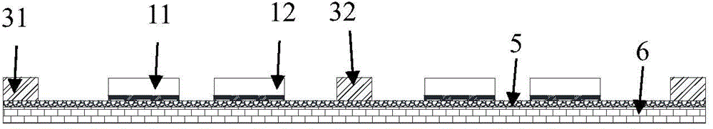
[0047] Step 110: paste the first chip 11, the second chip 12, the first height limiting block 31, and the second height limiting block 32 on the surface of the temporary bonding glue 5 of the carrier board 6;
[0048] Step 120: Cover the plastic sealing plate 7 on the first chip 11, the second chip 12, the first height limiting block 31 and the second height limiting block 32;
[0049] Step 130: filling the resin 4 into the first space, and curing to form an integral structure;
[0050] Step 140: removing the plastic sealing plate 7;
[0051] Step 150: remove the bearing plate 6 and the temporary bonding glue 5;
PUM
Abstract
The invention discloses a reconstruction wafer structure with a bared chip back and a manufacturing method thereof. The structure comprises a first chip, a second chip and a rewiring layer. Both the first chip and the second chip are arranged on the rewiring layer and have a first distance from the rewiring layer. The structure also comprises a first height limit block and a second height limit block which are arranged on the rewiring layer. The first height limit block and the second height limit block have a second distance from the rewiring layer. The first chip and the second chip are respectively arranged between the first height limit block and the second height limit block. A first space is formed by the rewiring layer, the first height limit block, the second height limit block, the first chip, and the second chip, and resin is filled in the first space. The second distance is equal to the first distance. According to the reconstruction wafer structure, through using the height limit blocks, the use of a high precision plastic mould is not needed, and the structure and the method have the technical effect of the great reduction of package manufacturing and processing cost.
Description
technical field [0001] The invention relates to the technical field of semiconductors, in particular to a reconfigured wafer structure and a manufacturing method with an exposed chip backside. Background technique [0002] With the development of large-scale integrated circuits, the lines are getting thinner and thinner. 22nm technology has entered mass production, and the thinning of lines has brought unprecedented challenges to equipment and processes. In order to improve the chip density and signalprocessing capability per unit area. With the continuous reduction of the line width and the enhancement of the signalprocessing capability, the chip size is continuously reduced, and the number of chip input and output pins is increasing, that is, the number of chip I / Os is increasing, and the large number of I / Os of a single chip As a result, the size of a single chipelectrode is also continuously reduced. The electrode size of the substrate is limited by processing and c...
Claims
Application Information
Patent Timeline
Application Date:The date an application was filed.
Publication Date:The date a patent or application was officially published.
First Publication Date:The earliest publication date of a patent with the same application number.
Issue Date:Publication date of the patent grant document.
PCT Entry Date:The Entry date of PCT National Phase.
Estimated Expiry Date:The statutory expiry date of a patent right according to the Patent Law, and it is the longest term of protection that the patent right can achieve without the termination of the patent right due to other reasons(Term extension factor has been taken into account ).
Invalid Date:Actual expiry date is based on effective date or publication date of legal transaction data of invalid patent.

