Failure analysis method for gate oxide defect original appearance

A technology for gate oxide layer and failure analysis, which is applied in the direction of electrical components, circuits, semiconductor/solid-state device testing/measurement, etc., and can solve problems such as unrecorded technical characteristics of gate oxide layer

Active Publication Date: 2014-10-01
WUHAN XINXIN SEMICON MFG CO LTD
View PDF7 Cites 20 Cited by
  • Summary
  • Abstract
  • Description
  • Claims
  • Application Information

AI Technical Summary

Problems solved by technology

[0008] The above two patents do not record the technical features related to the failure

Method used


Image

  • Failure analysis method for gate oxide defect original appearance
  • Failure analysis method for gate oxide defect original appearance
  • Failure analysis method for gate oxide defect original appearance

Examples


Embodiment Construction

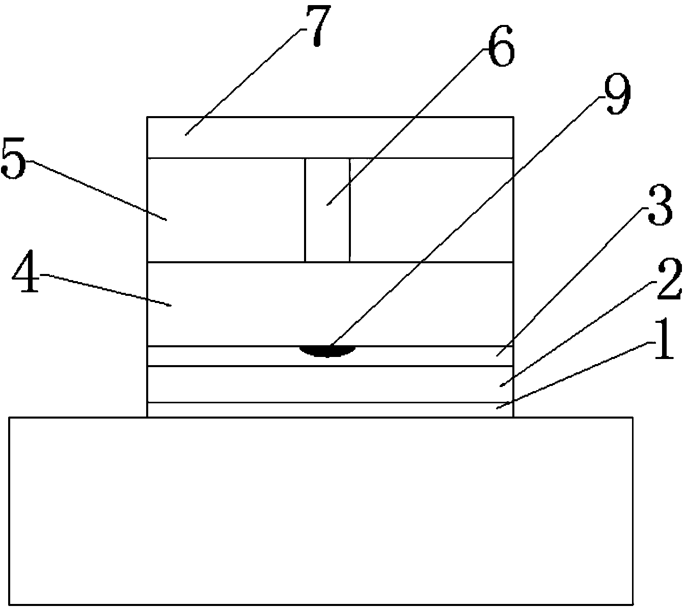
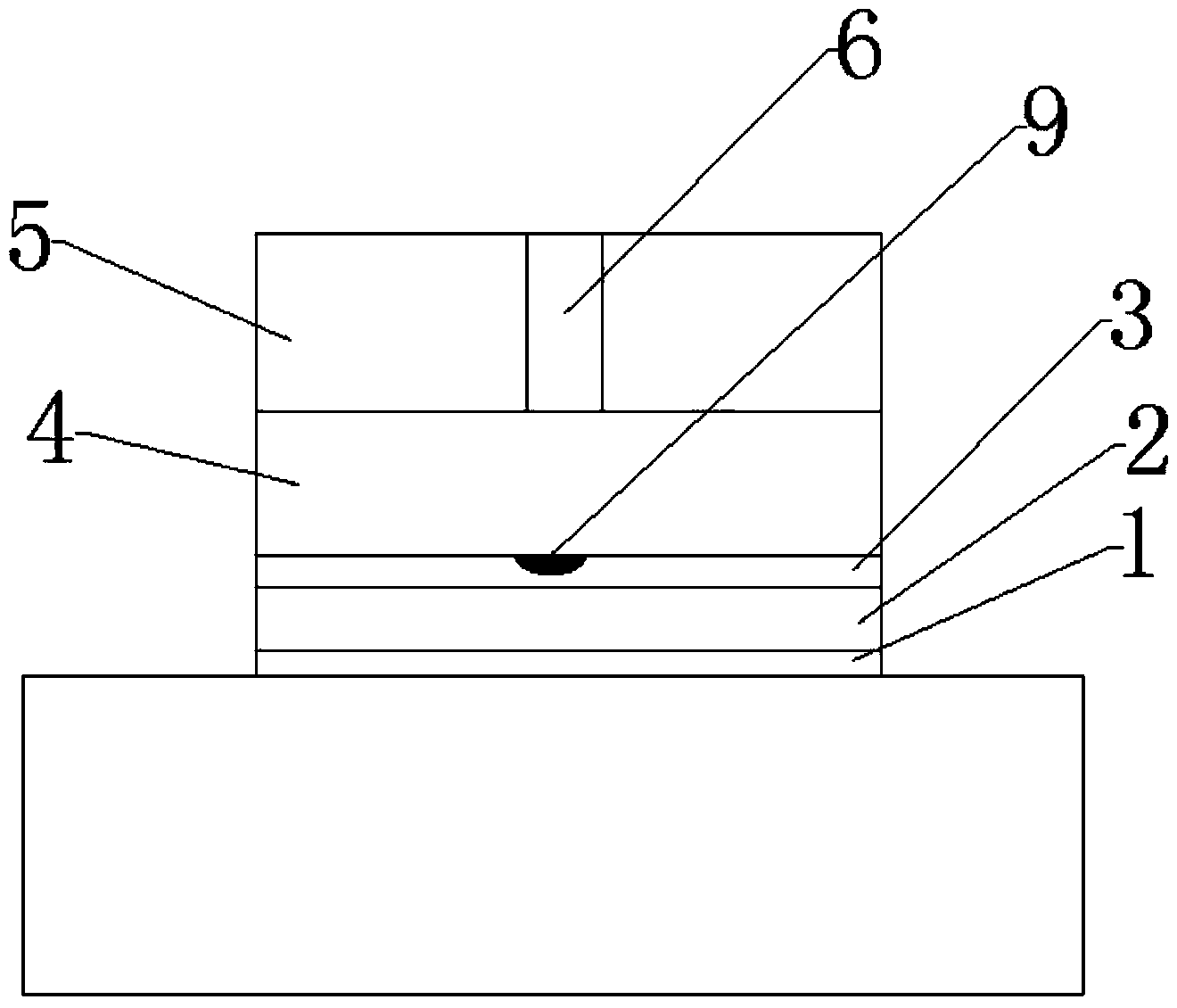
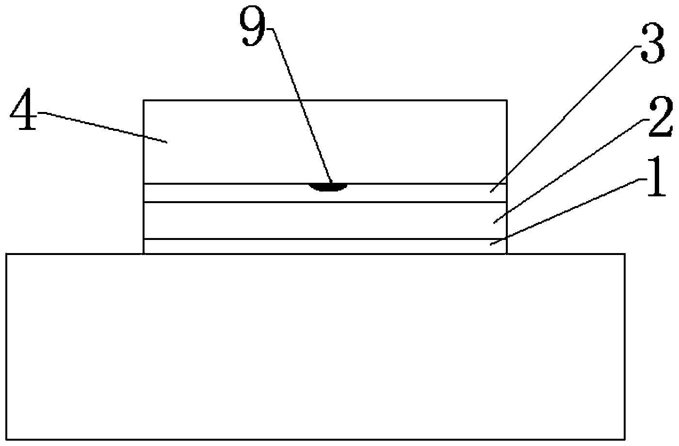
[0033] The present invention will be further described below in conjunction with the accompanying drawings and specific embodiments, but not as a limitation of the present invention. The invention relates to a method for analyzing the failure of the original appearance of gate oxide layer defects. Firstly, several semiconductor structures to be tested are provided with a gate structure and a metal interconnection layer located above the gate structure, and the gate structure includes a gate oxide layer, Gate 4 and interconnection 6, preferably, the gate oxide layer can be an oxide layer or an ONO dielectric layer. In order to explain the present invention more clearly, the present embodiment takes an ONO (Oxide Nitride Oxide) dielectric layer as an example, namely The above gate oxide layer includes a first oxide layer 1 , a nitride layer 2 and a second oxide layer 3 in sequence from bottom to top.

[0034] A preset voltage is applied to each semiconductor structure to be test...


PUM


Abstract

The invention relates to the technical field of semiconductor defect analysis, in particular to a failure analysis method for a gate oxide defect original appearance. The method includes the steps that firstly, a semiconductor structure to be tested is screened out under the preset voltage condition, wherein the semiconductor structure to be tested has a gate oxide defect; secondly, the semiconductor structure to be tested is operated, the semiconductor structure has the gate oxide defect, a metal interconnection layer is ground off, a scanning electron microscope voltage comparison method is used for determining the position of the gate oxide defect, an interconnection line, a dielectric layer and a gate are removed in sequence, a contrast layer having the high contrast ratio with the transmission electron microscope contrast ratio of the gate oxide is deposited on the rest of the gate oxide, a transmission electron microscope sample is manufactured on a defective gate area, and finally analysis is conducted through a transmission electron microscope. According to the failure analysis method for the gate oxide defect original appearance, the gate oxide defect original appearance can be clearly observed, and a forceful basis and a forceful direction can be provided for finding the processing technology defect of the gate oxide.

Description

technical field [0001] The invention relates to the technical field of semiconductor defect analysis, in particular to a failure analysis method for the original defect appearance of a gate oxide layer. Background technique [0002] The gate oxide breakdown voltage test (GOI / ONO Vramp) is a common method for evaluating the gate oxide process. The samples after the gate oxide breakdown voltage test usually have breakdown of the gate oxide layer, even if there is no breakdown , Breakdown will also occur during the subsequent failure analysis and location (grasp the hot spot) (only after the breakdown, the subsequent physical property analysis can observe the failure point, the resolution of the machine is limited, such as the resolution of the scanning electron microscope is more than a few tenths of a nanometer) . Therefore, the failure analysis of the existing breakdown voltage test of the gate oxide layer is basically the analysis of the condition after the breakdown of th...

Claims


Application Information

Patent Timeline
IPC IPC(8): H01L21/28H01L21/66
CPCH01L22/12
Inventor 李桂花仝金雨郭伟刘君芳李品欢
Owner WUHAN XINXIN SEMICON MFG CO LTD
Why Eureka
Try Eureka