Dual-pattern LED patterned substrate and LED chip

A patterned substrate and double-pattern technology, which is applied in the direction of electrical components, circuits, semiconductor devices, etc., can solve the problem of reducing the space for improving the LED light extraction rate of the patterned substrate, unfavorable nucleation and growth of epitaxial GaN crystals, and single pattern rules Problems such as permanent arrangement, to achieve the effect of weakening the side luminous flux, improving LED light output efficiency, and reducing the ratio of side luminous flux

Inactive Publication Date: 2014-10-01
SOUTH CHINA UNIV OF TECH
View PDF4 Cites 3 Cited by
  • Summary
  • Abstract
  • Description
  • Claims
  • Application Information

AI Technical Summary

Problems solved by technology

However, due to the limitations of the development of pattern etching technology, the pattern design of graphic substrate technology has been limited to the regular arrangement of a single pattern, such as the rectangular or hexagonal arrangement of a single pattern such as cones, hexagonal pyramids, triangular pyramids, and hemispheres.
In these traditional substrate pattern designs, the pattern spacing cannot be reduced infinitely. Even in the most densely arranged patterns, there are still many gaps between adjacent patterns, and this part of the gap will be greatly reduced. Small room for improving the light extraction rate of the graphics substrate LED
Moreover, an overly dense substrate pattern is not conducive to the nucleation and growth of epitaxial GaN crystals, so the design and arrangement of patterned substrate patterns is a major problem in optimizing the light extraction efficiency of LEDs.

Method used


Image

  • Dual-pattern LED patterned substrate and LED chip
  • Dual-pattern LED patterned substrate and LED chip
  • Dual-pattern LED patterned substrate and LED chip

Examples


Embodiment 1

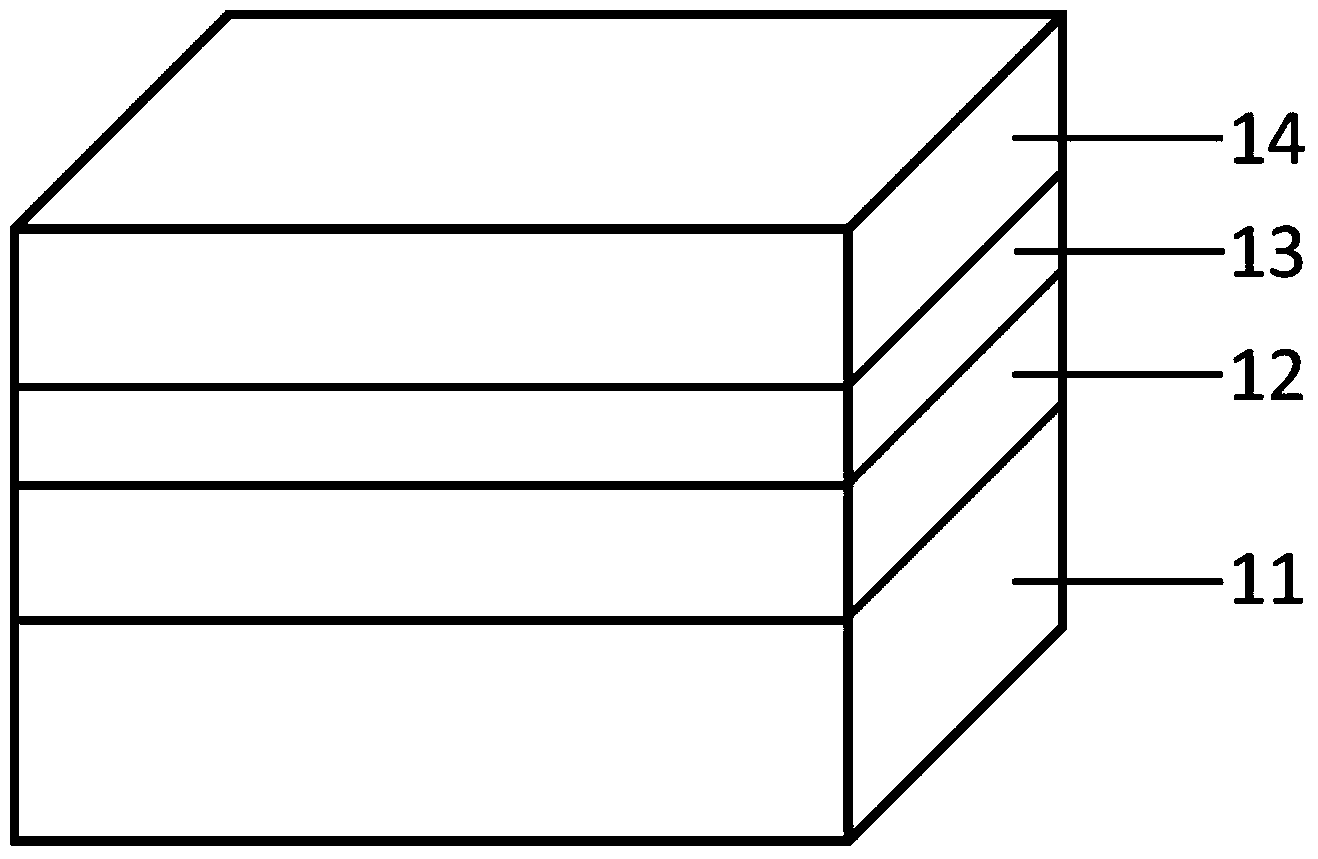
[0027] Such as figure 1 As shown, the LED chip of this embodiment is composed of a double-patterned LED patterned substrate 11 , an N-type GaN layer 12 , an MQW quantum well layer 13 , and a P-type GaN layer 14 .

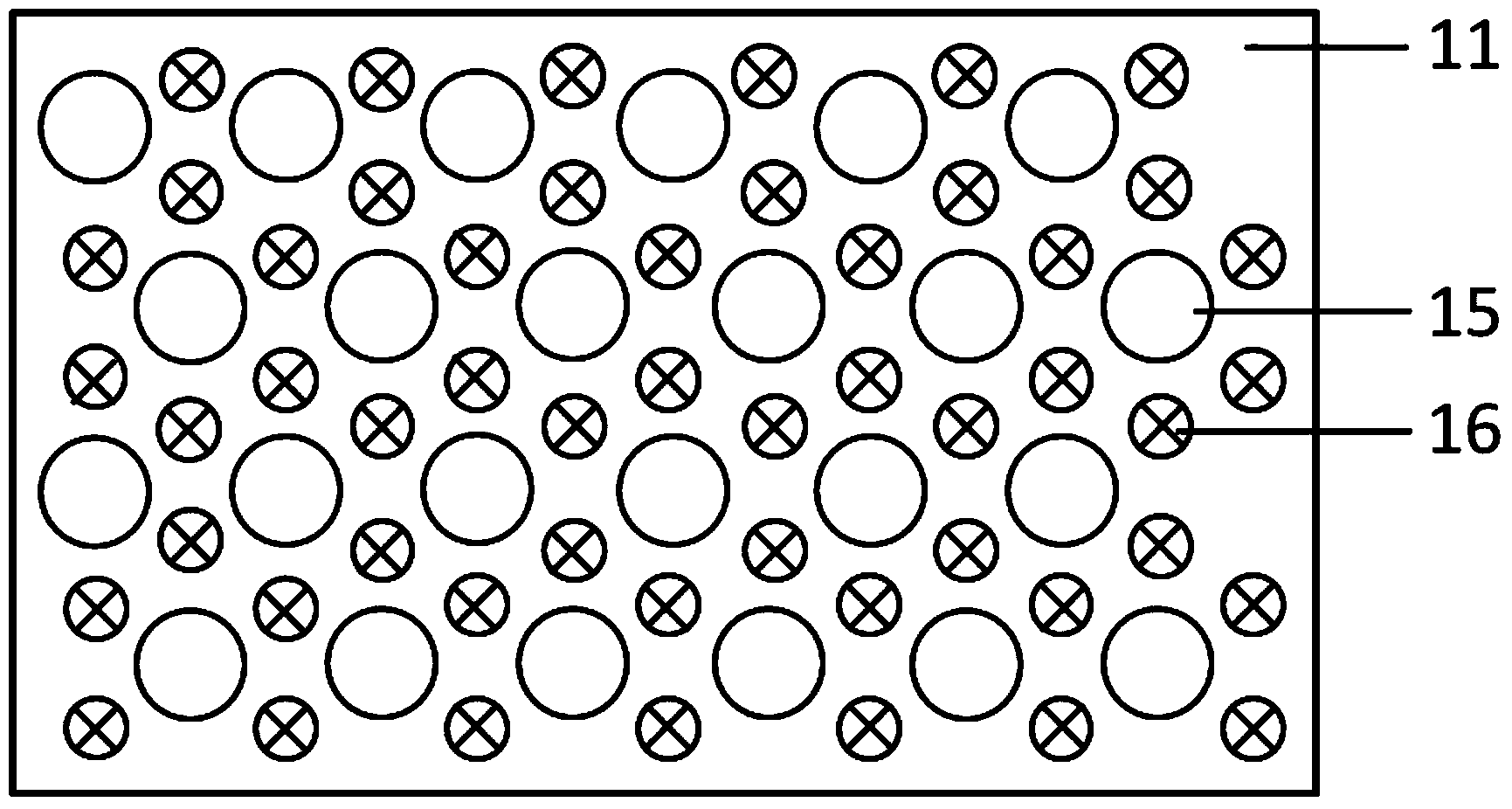
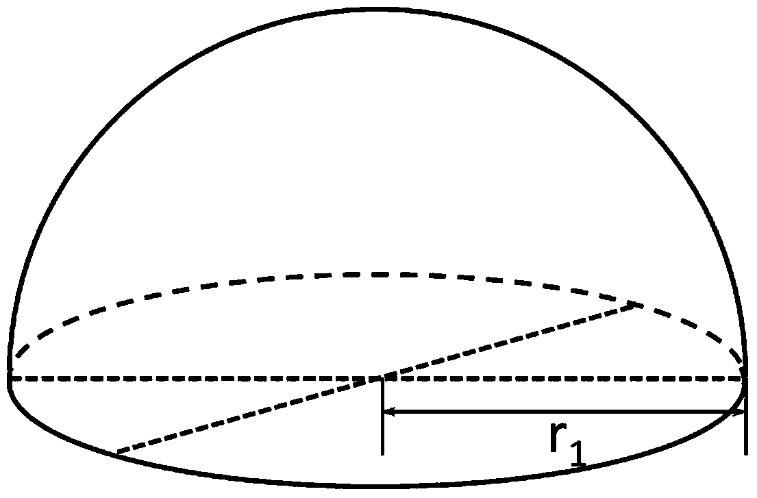
[0028] The double-patterned LED patterned substrate of this embodiment is as figure 2 As shown, the pattern on the substrate is composed of a hemispherical pattern 15 and a conical pattern 16 arranged on the substrate surface, and the radius of the bottom circle of the hemispherical pattern is r 1 is 1.0 μm, the distance d between adjacent hemispherical patterns is 3.0 μm, and the arrangement is hexagonal; the radius of the bottom circle of the conical pattern is r 2 0.4μm, inclination α 2 55°, arranged in the gap of the hemispherical pattern. Among them, the schematic diagram of the hemisphere pattern monomer is shown in image 3 , the schematic diagram of the cone pattern monomer is shown in Figure 4 .

[0029] The double-patterned LED patterned substrate ...

Embodiment 2

[0048] The LED chip of this embodiment is composed of a double-patterned LED patterned substrate, an N-type GaN layer, an MQW quantum well layer, and a P-type GaN layer arranged in sequence.

[0049] The pattern on the double-patterned LED patterned substrate of this embodiment consists of a hemispherical pattern and a conical pattern arranged on the surface of the substrate. The radius of the bottom circle of the hemispherical pattern is 1.0 μm, the distance between adjacent hemispherical patterns is 3.0 μm, and the arrangement is hexagonal; in the gap.

[0050] The double-patterned LED patterned substrate of the present embodiment is simulated and tested:

[0051] The optical analysis software TracePro is used to perform a simulation test on the patterned substrate of the LED chip of this embodiment. The simulation test process is as follows:

[0052] (1) Substrate construction: The modeling function of TracePro is used to realize the fabrication of the substrate. The size...

Embodiment 3

[0064] The LED chip of this embodiment is composed of a double-patterned LED patterned substrate, an N-type GaN layer, an MQW quantum well layer, and a P-type GaN layer arranged in sequence.

[0065] The double-patterned LED patterned substrate of this embodiment is as Figure 5 As shown, the pattern on the substrate 21 is composed of a hemispherical pattern 25 and a conical pattern 26 arranged on the substrate surface, and the radius of the bottom circle of the conical pattern is r 2 1.0μm, inclination α 3 is 55°, the distance d between adjacent conical patterns is 3.0 μm, and the arrangement is rectangular; the radius of the bottom circle of the hemispherical pattern is r 1 0.4 μm, arranged in the gap of the cone pattern.

[0066] The double-patterned LED patterned substrate of the present embodiment is simulated and tested:

[0067] Adopt optical analysis software TracePro to do simulation test to the patterned substrate of LED chip of the present invention, simulation t...


PUM


Abstract

The invention discloses a dual-pattern LED patterned substrate. Patterns on the substrate include the hemispherical pattern and the conical pattern. The radius r1 of the bottom circle of the hemispherical pattern is not equal to the radius r2 of the bottom circle of the conical pattern. The invention further discloses an LED chip comprising the dual-pattern LED patterned substrate. The light emitting efficiency of an LED is improved through the combination with the effect of the conical surface of the conical pattern and the spherical surface of the hemispherical pattern on optimizing the LED light emitting efficiency; the patterns on the substrate are dense, and therefore more light rays can be emitted out of the LED chip, especially, more light rays can be emitted out of the top and the bottom of the chip, and the LED light extraction ratio is greatly increased.

Description

technical field [0001] The invention relates to an LED patterned substrate, in particular to a double-pattern LED patterned substrate and an LED chip. Background technique [0002] In recent years, GaN-based LEDs have been widely used in traffic lights, LCD backlights, full-color displays, and general lighting due to their advantages such as high brightness, low energy consumption, and long life. However, there is a huge difference between the refractive index of GaN material (n=2.45) and air (n=1.0), and the critical angle of total reflection is only about 24°, which leads to the significant total reflection of light inside the chip and cannot be emitted. LED, which greatly reduces the light extraction rate of the LED. Later, improvement schemes were proposed for this problem, such as introducing Bragg reflection layer, photonic crystal, surface roughening and substrate patterning, etc. Among them, the patterned substrate technology can not only improve the light extracti...

Claims


Application Information

Patent Timeline
Patent Type & Authority Applications(China)
IPC IPC(8): H01L33/24
CPCH01L33/20
Inventor 李国强王海燕林志霆周仕忠乔田王凯诚钟立义
Owner SOUTH CHINA UNIV OF TECH
Why Eureka
Try Eureka