
Straight-through motherboard socket and manufacturing method thereof

A motherboard and socket technology, applied in the direction of coupling devices, electrical components, connections, etc., can solve the problems that cannot be reduced, the manufacturing process is laborious and time-consuming, and the opening area cannot be reduced, so as to achieve the effect of reducing the area and high-density installation

Inactive Publication Date: 2016-08-17
SMK CO LTD
View PDF6 Cites 0 Cited by
  • Summary
  • Abstract
  • Description
  • Claims
  • Application Information

AI Technical Summary

Problems solved by technology

However, the strength of the side wall 101b of the insulating case 101 is required to fix and support the contacts 103 and the side sealing plate 104. Therefore, there is a limit to its thinning, and the wall of the side sealing plate 104 or the bottom sealing plate 105 cannot be added. Thick outer diameter D' shrinks
As a result, the opening area of ​​the mounting hole 111 falling into the through-board socket 100 cannot be reduced, which is an obstacle to high-density mounting of more electronic components on the printed circuit board 110.
[0012] Furthermore, due to the structural reason that the plurality of contacts 3 penetrate through the side wall portion 101b and are fixed, it is necessary to assemble the side sealing plate 104 and the bottom sealing plate 105 from the upper and lower directions of the insulating case 101 to seal the periphery of the electronic component receiving recess 102, At least two different types of sealing components are required, and at the same time, after fixing the plurality of contacts 3 to the side wall portion 101b, the side sealing plate 104 and the bottom sealing plate 105 of the at least two types of sealing components are assembled to the insulating case 101, and the respective The grounding legs 104c, 105a of the printed circuit board 110 are soldered and connected to the grounding pattern of the printed circuit board 110. Such an assembly and manufacturing process is very laborious and time-consuming.

Method used


Image

  • Straight-through motherboard socket and manufacturing method thereof
  • Straight-through motherboard socket and manufacturing method thereof
  • Straight-through motherboard socket and manufacturing method thereof

Examples


Embodiment Construction

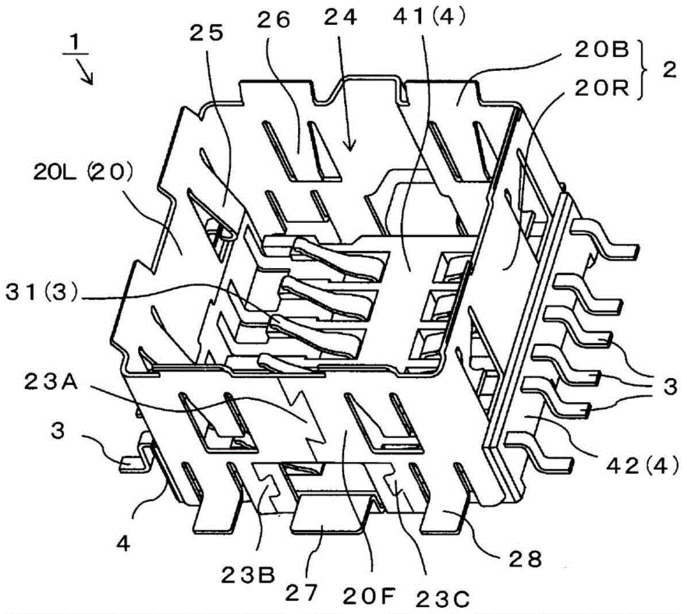
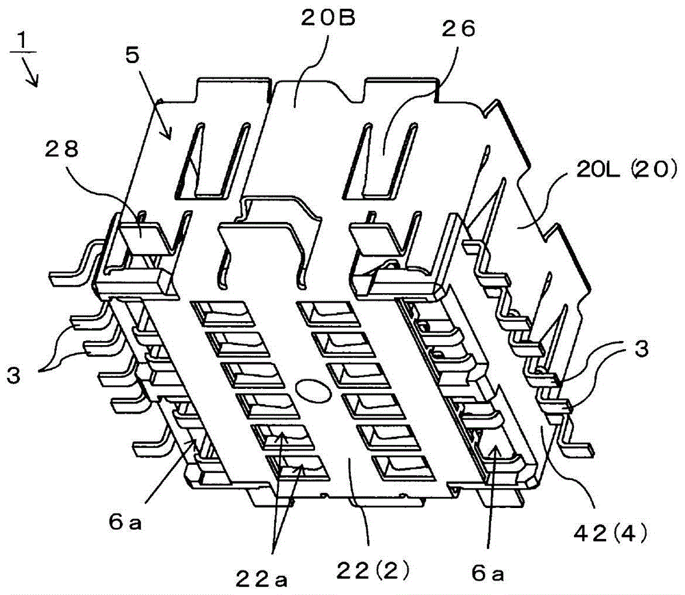
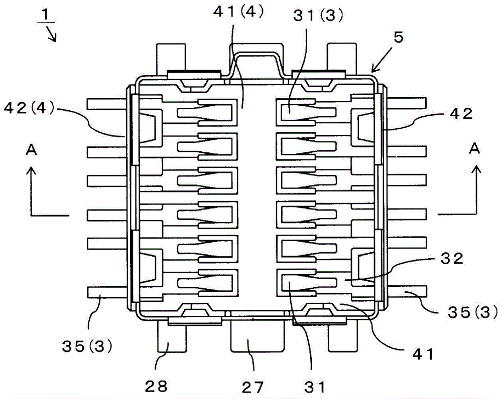
[0103] Refer below Figure 1 to Figure 9 The pass-through motherboard socket 1 and its manufacturing method related to an embodiment of the present invention will be described. The embodiments described below are suitable specific examples of the present invention. Although various technical limitations are made on the constituent elements, types, combinations, shapes, relative configurations, etc., these are merely examples, and the present invention is not limited thereto. .

[0104] The through motherboard socket 1 is installed in the housing of the portable telephone Figure 4 The mounting hole 121 of the printed circuit board 120 is used to connect the camera module (not shown) stored in the upper part of the figure to the printed circuit board 120, and connect the parts of the main board socket 1 on the lower side. In the description, Figure 4 The directions shown are the up, down, left, and right directions. Figure 4 The paper faces the inside direction as the back and ...


PUM


Abstract

The invention relates to a through-motherboard socket and a manufacturing method thereof. The side sealing plate is provided with an opening at the position where the plurality of contacts are inserted through, and the plurality of contacts are inserted through the opening, so that the side sealing plate and the plurality of contacts are integrally formed with the insulating housing covering at least a part of the opening, and the plurality of contacts are inserted into the opening. The contacts are insulated from the side sealing plates, supported in the insulating housing. A plurality of contacts are integrally formed with the insulating case, so they can be supported by a thin-walled insulating case, and at the same time, supported at a portion of the insulating case that does not overlap the wall thickness of the side sealing plate and covers the opening of the side sealing plate Therefore, the plurality of contacts can shorten the outer diameter (D) of the straight-through mainboard socket in the direction of insertion of the contacts, thereby reducing the installation area. Provided is a through-board socket capable of reducing the mounting area for mounting on a printed wiring board and enabling high-density mounting on a printed wiring board, and a method for manufacturing the same.

Description

Technical field [0001] The present invention relates to a through board socket that connects a rectangular parallelepiped electronic component such as a camera module to a printed circuit wiring board and a method of manufacturing the same. More specifically, it relates to a through board socket mounted in a through printed wiring board. Straight-through motherboard socket and its manufacturing method. Background technique [0002] When assembling a rectangular parallelepiped-shaped electronic component with a certain height such as a camera module into a thin electronic device such as a portable telephone, drop the part below the through-board socket into the mounting hole of the printed circuit board that penetrates the electronic device , The electronic components are stored in the electronic component accommodating portion opened above the through-board socket, and connected to the printed circuit board (see Patent Document 1). [0003] Below, refer to Figure 11 to Figure 14 T...

Claims


Application Information

Patent Timeline
Patent Type & Authority Patents(China)
IPC IPC(8): H01R13/502H01R43/20
Inventor 大泽文雄宇留鹫修一
Owner SMK CO LTD
Learn More