Single-chip optical path module and multi-die semiconductor laser

A single-chip, semiconductor technology, applied in the field of lasers, can solve the problems of inability to guarantee the repeatability and stability of the chip product process, the poor versatility of unit devices, and the consumption of material and manpower, so as to achieve mass production, simplify rework, and save time. and cost effects

Inactive Publication Date: 2014-10-22
BWT BEIJING
View PDF7 Cites 5 Cited by
  • Summary
  • Abstract
  • Description
  • Claims
  • Application Information

AI Technical Summary

Problems solved by technology

Since the CoS is welded on the bottom plate, if one fails, it needs to be replaced again, and the bottom plate is made of metal with high thermal conductivity. During the process of replacing the CoS, other unit devices will be affected, and they need to be adjusted again. Due to the poor detachability, the space integration method of all unit devices on the same base plate leads to poor versatility of unit devices, and cannot guarantee the process repeatability and stability of different chip products, which consumes a lot of material and manpower

Method used


Image

  • Single-chip optical path module and multi-die semiconductor laser
  • Single-chip optical path module and multi-die semiconductor laser
  • Single-chip optical path module and multi-die semiconductor laser

Examples


Embodiment Construction

[0040] In order to make the object, technical solution and advantages of the present invention clearer, the implementation manner of the present invention will be further described in detail below in conjunction with the accompanying drawings.

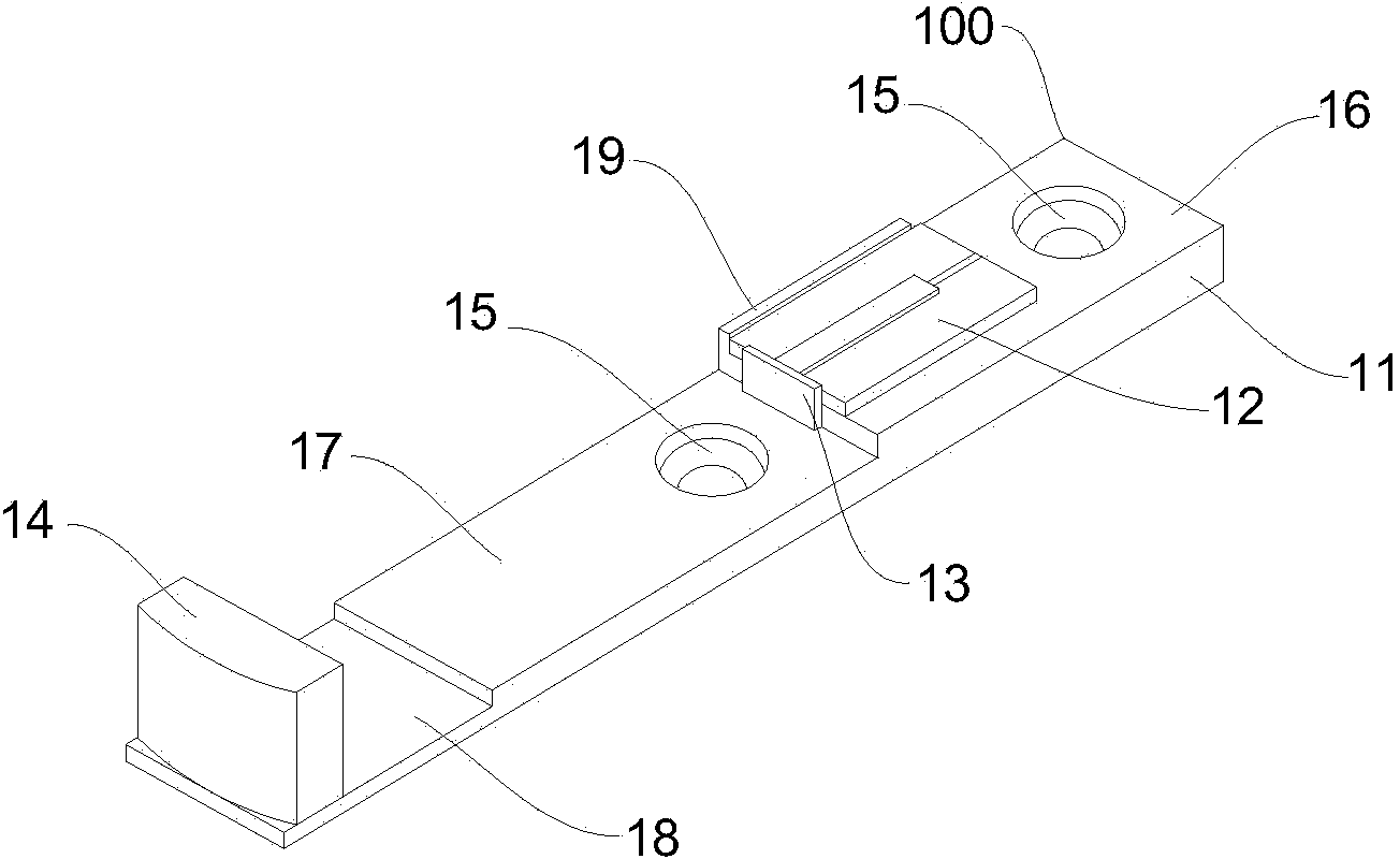
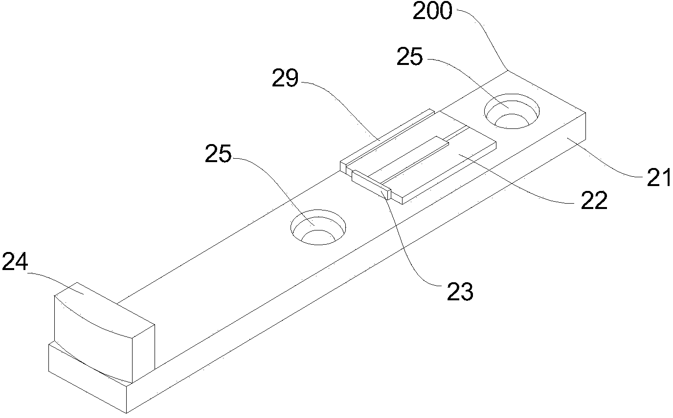
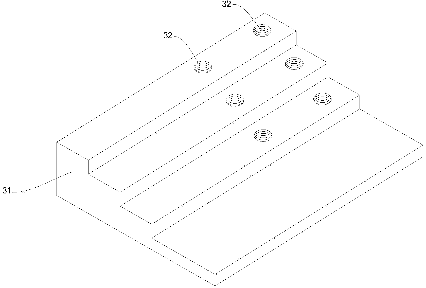
[0041] In the present invention, multiple semiconductor laser unit devices in a multi-die semiconductor laser are respectively modularized to form a plurality of single-chip optical path modules, and the single-chip optical path module is detachably fixed on the stepped bottom plate of the multi-die semiconductor laser. , so as to solve the problem of commonality of components of different multi-chip laser products, and simplify the rework and rework procedures, saving time and cost.

[0042] Embodiment 1 of a single-chip optical circuit module

[0043] figure 1 It is a structural schematic diagram of Embodiment 1 of the single-chip optical path module in the present invention. Such as figure 1 As shown, this embodiment discloses a ...


PUM


Abstract

The invention relates to the technical field of laser, and particularly relates to a single-chip optical path module and a multi-die semiconductor laser. The single-chip optical path module comprises a heat sink module, a semiconductor laser chip CoS with auxiliary heat sink, a fast axis collimating lens and a slow axis collimating lens. The CoS, the fast axis collimating lens and the slow axis collimating lens are sequentially fixed on one surface of the heat sink module; and the optical axis of the output beam of the CoS, and the optical axis of the fast axis collimating lens and the optical axis of the slow axis collimating lens are in the same line. The multi-die semiconductor laser comprises a step-shaped bottom board and the plurality of single-chip optical path modules, wherein the plurality of single-chip optical path module are fixed to the different steps of the step-shaped bottom board respectively. According to the single-chip optical path modules and the multi-die semiconductor laser, modularization of a plurality of single-chip optical paths are realized; in the multi-die semiconductor laser, the single-chip optical path modules can be fixed in a detachable manner, so that different lasers are allowed to use one type of module; and process repeatability and stability are improved.

Description

technical field [0001] The invention relates to the field of laser technology, in particular to a single-chip optical path module and a multi-tube core semiconductor laser. Background technique [0002] In current multi-die semiconductor lasers, all semiconductor laser chips (CoS) with auxiliary heat sinks are usually welded on the same base plate by metal solder, and then the optical elements are fixed on the base plate to collimate the single optical path. The other end of the fixed reflection unit turns each collimated beam, and then focuses and couples them together through the lens. Since the CoS is welded on the bottom plate, if one fails, it needs to be replaced again, and the bottom plate is made of metal with high thermal conductivity. During the process of replacing the CoS, other unit devices will be affected, and they need to be adjusted again. However, this kind of spatial integration of all unit devices on the same base plate leads to poor versatility of unit ...

Claims


Application Information

Patent Timeline
Patent Type & Authority Applications(China)
IPC IPC(8): H01S5/022H01S5/024
Inventor 杨朝栋姜笑尘刘瑞高燕燕何晓光
Owner BWT BEIJING
Why Eureka
Try Eureka