Method for Constraining Safe Operating Area Trajectories of Power Semiconductor Devices
A technology of power semiconductor and safe working area, applied in semiconductor devices, electric solid state devices, instruments, etc., can solve the problem that the peak power is not significantly constrained
- Summary
- Abstract
- Description
- Claims
- Application Information
AI Technical Summary
Problems solved by technology
Method used
Image
Examples
Embodiment Construction
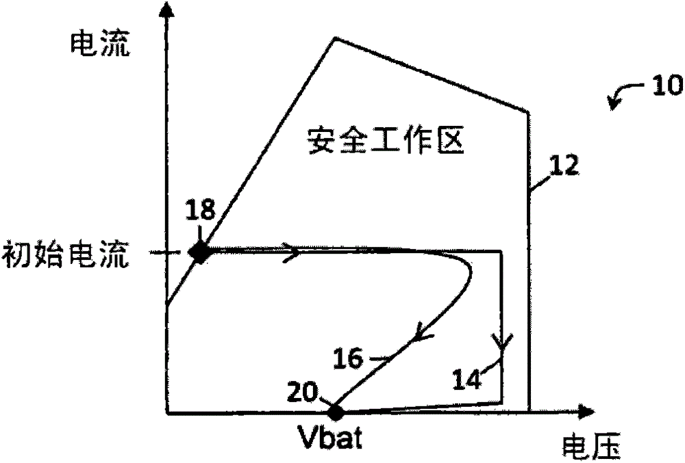
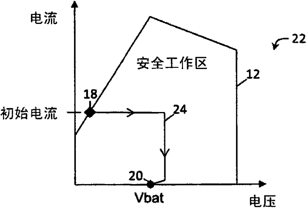
[0033] now refer to figure 2 , the positive offset safe operating area (SOA) trajectory 12 for the maximum ratio of the power semiconductor device is shown in graph 22 . As noted above, the SOA locus 12 represents the maximum simultaneous source-drain voltage and drain current that the power MOSFET can safely handle. In an embodiment of the present invention, the SOA trace 12 is constrained into a constrained SOA trace 24 with an N-channel enhancement mode power MOSFET in a high-side configuration between the power supply and the load. Those skilled in the art will appreciate that graph 22 may depict SOA trajectories for other devices, such as BJTs. Nevertheless, it can be seen that the source-drain voltage of the power MOSFET is constrained and the peak power generation as well as the total energy absorption of the power MOSFET is constrained to minimize the use of the SOA of the power MOSFET.
[0034] Constrained SOA trajectory 24 is generated according to the method desc...
PUM
 Abstract
Description
Claims
Application Information


