Semiconductor device and manufacturing method thereof

A device manufacturing method and semiconductor technology, applied in the fields of semiconductor/solid-state device manufacturing, semiconductor devices, semiconductor/solid-state device components, etc., can solve the problems affecting the improvement of device performance, difficulty in manufacturing large-scale devices, and low resistivity, etc. Achieve the effect of improving device reliability and reducing source-drain contact resistance

Active Publication Date: 2019-03-15
INST OF MICROELECTRONICS CHINESE ACAD OF SCI
View PDF6 Cites 0 Cited by
  • Summary
  • Abstract
  • Description
  • Claims
  • Application Information

AI Technical Summary

Problems solved by technology

In this way, most of the contact plugs are made of metals W and Ti with high resistivity, which makes the contact plug resistance large and affects the improvement of device performance.
[0007] On the other hand, due to the narrow size of the contact hole, the filling rate of other commonly used low-resistance filling metals Cu and Al is low, and it is easy to form pores in the contact hole, which reduces the contact reliability.
However, Ag and Au, which have better ductility and lower resistivity, are difficult to use in large-scale device manufacturing due to their high price.

Method used


Image

  • Semiconductor device and manufacturing method thereof
  • Semiconductor device and manufacturing method thereof
  • Semiconductor device and manufacturing method thereof

Examples


Embodiment Construction

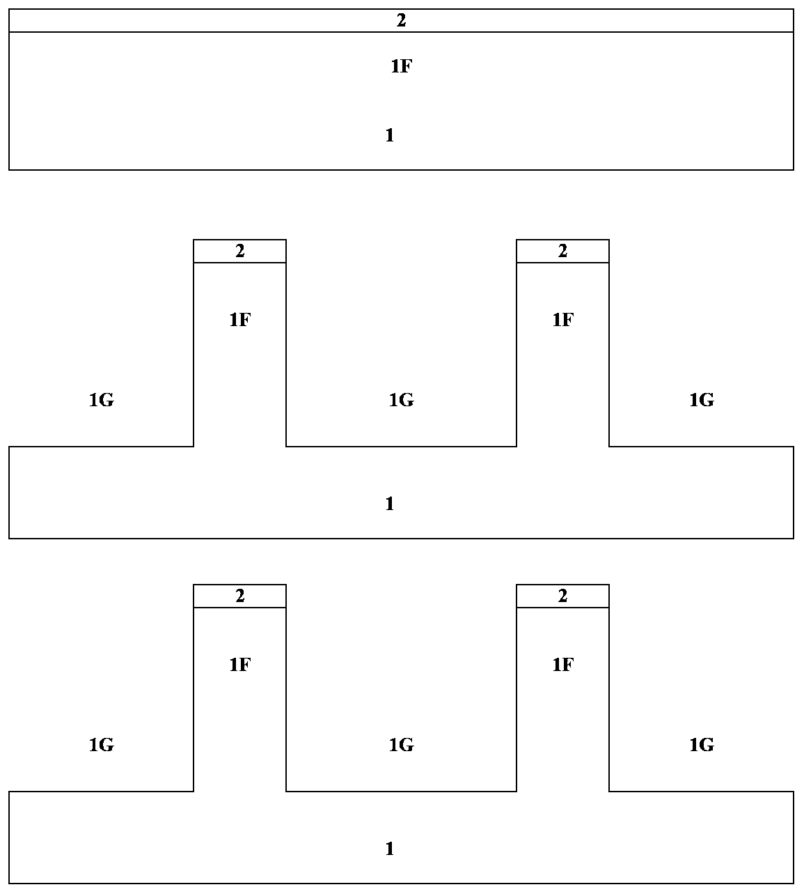
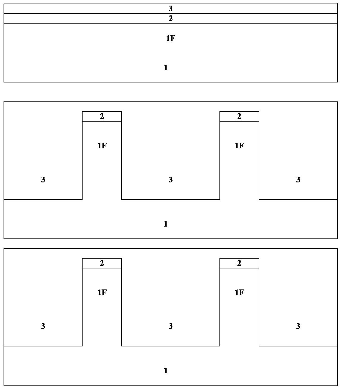
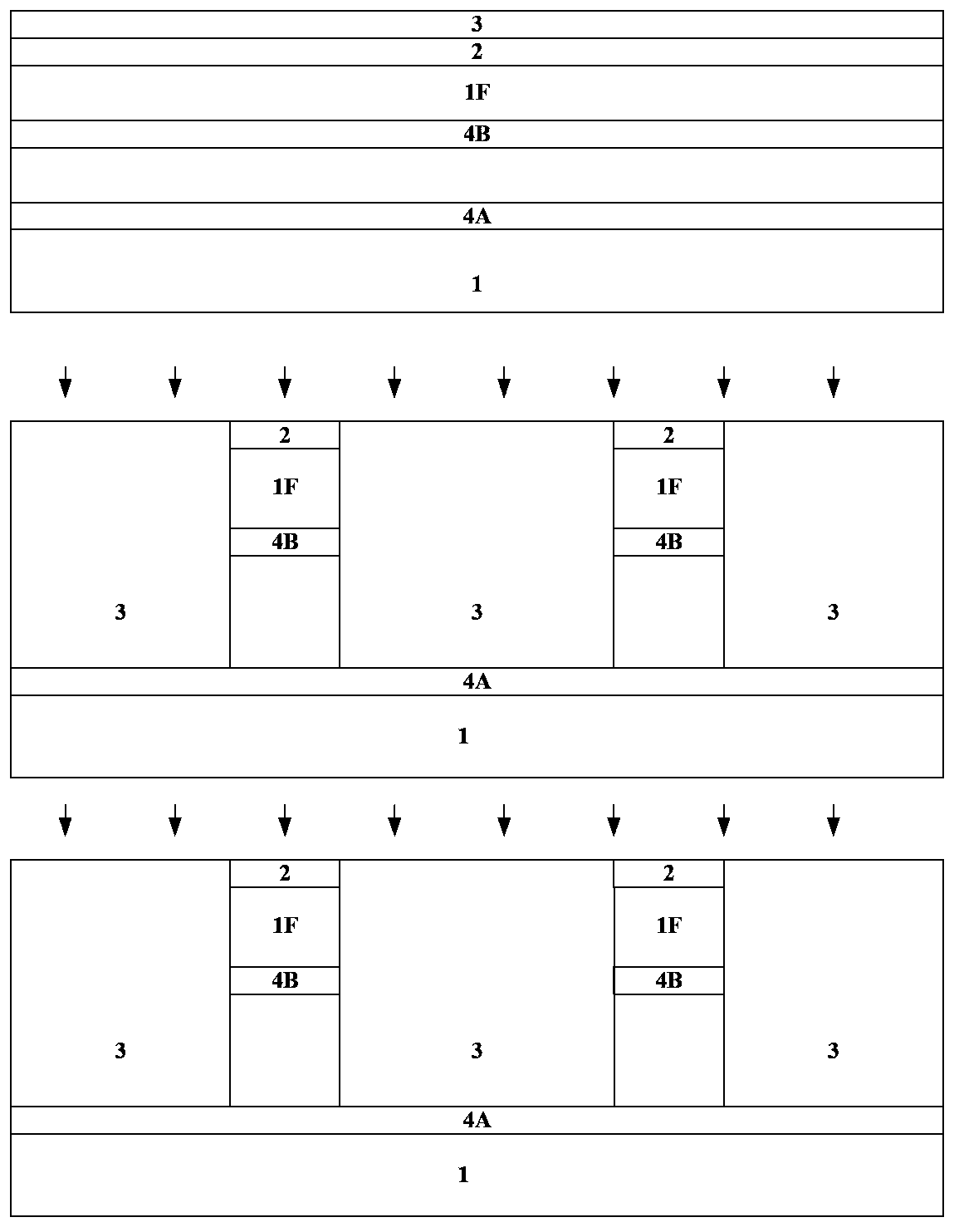
[0029] The characteristics and technical effects of the technical solution of the present invention will be described in detail below with reference to the accompanying drawings and in conjunction with schematic embodiments, and a three-dimensional multi-gate FinFET and its manufacturing method that can effectively reduce the source-drain contact resistance and simultaneously improve device reliability are disclosed. . It should be pointed out that similar reference numerals represent similar structures, and the terms "first", "second", "upper", "lower" and the like used in this application can be used to modify various device structures or manufacturing processes . These modifications do not imply spatial, sequential or hierarchical relationships of the modified device structures or fabrication processes unless specifically stated.

[0030] It is worth noting that the upper part of each of the following figures is the device along the Figure 15 The cross-sectional view of ...


PUM


Abstract

The invention discloses a semiconductor device and a manufacturing method thereof. The semiconductor device comprises a substrate, a gate on the substrate and source and drain regions at two sides of the gate. A first contact metal layer is formed on the source and drain region, and the top face of the first contact metal layer is lower than the top face of the gate. A second contact metal layer is formed on the first contact metal layer and the top face of the second contact metal layer is higher than the top face of the gate. According to the semiconductor device and the manufacturing method thereof, lower first contact metal layers are formed at two sides of a false gate, low-resistance second contact metal layers are formed on the first contact metal layers after the false gate is removed, source and drain contact resistance can be effectively reduced, and device reliability is improved.

Description

technical field [0001] The invention relates to a semiconductor device and a manufacturing method thereof, in particular to a three-dimensional multi-gate FinFET capable of easily realizing a self-aligned contact structure with low resistivity and a manufacturing method thereof. Background technique [0002] In the current sub-20nm technology, the three-dimensional multi-gate device (FinFET or Tri--gate) is the main device structure, which enhances the gate control ability and suppresses leakage and short channel effects. [0003] For example, compared with traditional single-gate bulk Si or SOI MOSFETs, MOSFETs with double-gate SOI structures can suppress short-channel effects (SCE) and drain-induced barrier lowering (DIBL) effects, have lower junction capacitance, and can To achieve light channel doping, the threshold voltage can be adjusted by setting the work function of the metal gate, which can obtain about 2 times the driving current and reduce the requirements for th...

Claims


Application Information

Patent Timeline
Patent Type & Authority Patents(China)
IPC IPC(8): H01L21/336H01L21/768H01L29/78H01L23/528
Inventor 殷华湘朱慧珑
Owner INST OF MICROELECTRONICS CHINESE ACAD OF SCI
Why Eureka
Try Eureka