Super junction lateral double diffusion metal oxide semiconductor field effect transistor and manufacturing method thereof

An oxide semiconductor and lateral double-diffusion technology, which is applied in semiconductor/solid-state device manufacturing, semiconductor devices, electrical components, etc., can solve problems such as reducing the lateral breakdown voltage of SJ-LDMOS, and achieve high lateral and vertical breakdown voltages, Effect of High Lateral Breakdown Voltage

Inactive Publication Date: 2014-10-29
HOOYI SEMICON +1
View PDF4 Cites 12 Cited by
  • Summary
  • Abstract
  • Description
  • Claims
  • Application Information

AI Technical Summary

Problems solved by technology

[0005] The invention provides a super-junction lateral double-diffused metal oxide semiconductor field effect transistor and its manufacturing method, which are used to solve the

Method used


Image

  • Super junction lateral double diffusion metal oxide semiconductor field effect transistor and manufacturing method thereof

Examples


Embodiment 1

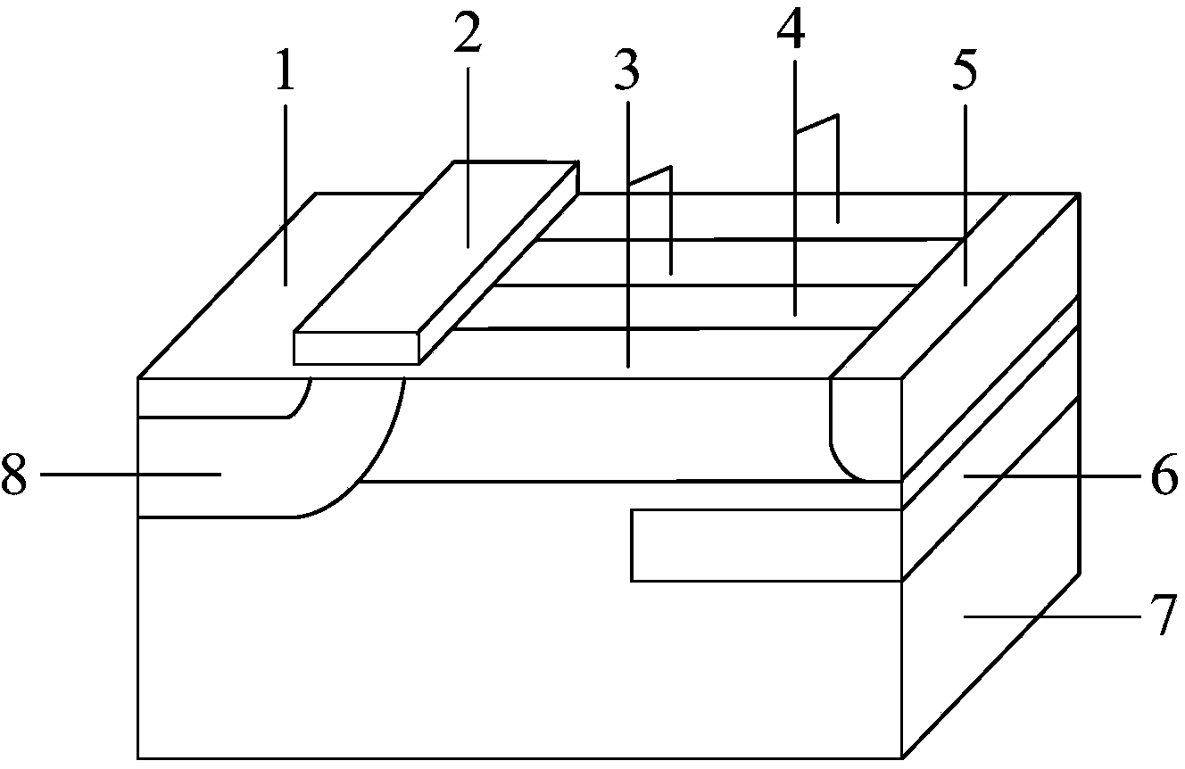
[0025] like figure 1 As shown, the present invention provides a super junction lateral double diffused metal oxide semiconductor field effect transistor, referred to as SJ-LDMOS, which includes a P-type semiconductor substrate 7 and an active region and a gate region 2 formed on the surface of the semiconductor substrate 7 . The active region includes an N-type source region 1, an N-type drain region 5, a P-type base region 8 and a lateral super junction structure. Wherein, the base region 8 serves as a channel of the MOS transistor, the source region 1 is formed in the base region 8 , and the source region 1 and the drain region 5 are located on both sides of the gate region 2 . The lateral superjunction structure includes N-type pillar regions 3 and P-type pillar regions 4 arranged alternately in the lateral direction. The heavily doped N-type pillar regions 3 and P-type pillar regions 4 reduce the on-resistance of SJ-LDMOS and minimize the conduction loss change.

[0026...

Embodiment 2

[0041] Based on the same inventive concept, the present invention also provides a method for fabricating the SJ-LDMOS in Embodiment 1, including the step of forming an active region and a gate region on the surface of a semiconductor substrate of the first conductivity type, the forming The steps for the source zone include:

[0042] forming a base region of a first conductivity type in the semiconductor substrate;

[0043]forming a source region of a second conductivity type in the base region;

[0044] forming a drain region of a second conductivity type in the semiconductor substrate, the source region and the drain region being located on both sides of the gate region;

[0045] Formed between the base region and the drain region, the lateral super junction structure includes N-type pillar regions and P-type pillar regions alternately arranged laterally.

[0046] The step of forming the active region also includes:

[0047] A buried region of the second conductivity type...


PUM


Abstract

The invention relates to the field of semiconductor devices and discloses a super junction lateral double diffusion metal oxide semiconductor (SJ-LDMOS) field effect transistor and a manufacturing method thereof. An active area of the SJ-LDMOS comprises a lateral super junction structure and a burying area formed below the lateral super junction structure. Due to the fact that the conduction types of the burying area and the semiconductor substrate are different, the semiconductor substrate and the burying area can assist depletion of an N-type column area and a P-type column area of the lateral super junction structure, load unbalance between the N-type column area and the P-type column area caused by the substrate auxiliary effect is supplemented, and high lateral breakdown voltage can be obtained. Meanwhile, a P junction and an N junction between the semiconductor substrate and the burying area lead a high electric field peak towards the surface of the semiconductor substrate and in the vertical direction, even lateral and vertical electric field distribution can be achieved through the electric field modulation effect, and higher lateral and vertical breakdown voltage can be obtained.

Description

technical field [0001] The invention relates to the field of semiconductor devices, in particular to a superjunction lateral double-diffused metal oxide semiconductor field effect transistor and a manufacturing method thereof. Background technique [0002] Lateral Double-diffused MOSFET (LDMOS for short) has become a key device in the design of intelligent power integrated circuits and system-on-chips due to its advantages such as easy integration with low-voltage devices. Its main feature is that a relatively long lightly doped drift region is added between the base region and the drain region. The doping type of the drift region is consistent with that of the drain region. By adding the drift region, it can share the breakdown voltage. Improve the breakdown voltage of LDMOS. The optimization goal of LDMOS is low on-resistance, which minimizes conduction losses. [0003] The super junction (super junction) structure is alternately arranged N-type pillar regions and P-type...

Claims


Application Information

Patent Timeline
IPC IPC(8): H01L29/78H01L29/06H01L29/08H01L21/336
CPCH01L29/0623H01L29/0634H01L29/66681H01L29/7816H01L29/1083
Inventor 段宝兴袁小宁董超范玮朱樟明杨银堂
Owner HOOYI SEMICON
Why Eureka
Try Eureka