Organic light-emitting device and preparation method thereof
An electroluminescent device and luminescence technology, which is applied in the direction of electric solid-state devices, semiconductor/solid-state device manufacturing, electrical components, etc., can solve the problems of poor cathode electron injection ability, poor device stability, device luminous efficiency, and low light extraction performance, etc. problem, to achieve the effect of improving photon utilization rate, easy film formation, improving conductivity and light reflectivity
- Summary
- Abstract
- Description
- Claims
- Application Information
AI Technical Summary
Problems solved by technology
Method used
Image
Examples
Embodiment 1
[0063] A method for preparing an organic electroluminescent device, comprising the following steps:
[0064] (1) Ultrasonic cleaning of the ITO glass substrate with detergent and deionized water for 15 minutes each to obtain a clean conductive anode glass substrate;
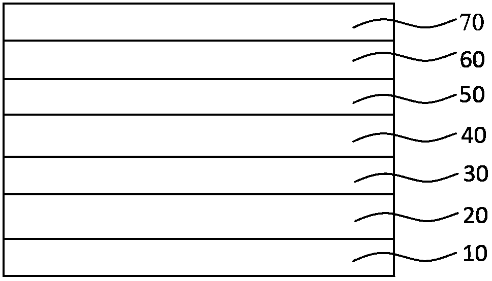
[0065] (2) In the high vacuum coating system (Shenyang Scientific Instrument Development Center Co., Ltd.), the pressure is 8×10 -5 Under the condition of Pa, on a clean conductive anode glass substrate, thermally resistively evaporated hole injection layer, hole transport layer, light emitting layer, electron transport layer and electron injection layer in sequence;
[0066] Specifically, in this embodiment, the material of the hole injection layer is WO 3 , with a thickness of 35nm; the material of the hole transport layer is NPB, with a thickness of 40nm; the material of the light-emitting layer is Alq3, with a thickness of 20nm; the material of the electron transport layer is Bphen, with a thickness of 80nm;...
Embodiment 2
[0073] A method for preparing an organic electroluminescent device, comprising the following steps:
[0074] (1) Ultrasonic cleaning of the AZO glass substrate with detergent and deionized water for 15 minutes each to obtain a clean conductive anode glass substrate;
[0075] (2) In the high vacuum coating system (Shenyang Scientific Instrument Development Center Co., Ltd.), the pressure is 2×10 -3 Under the condition of Pa, on a clean conductive anode glass substrate, thermally resistively evaporated hole injection layer, hole transport layer, light emitting layer, electron transport layer and electron injection layer in sequence;
[0076] Specifically, in this embodiment, the material of the hole injection layer is MoO 3 , with a thickness of 80nm; the material of the hole transport layer is NPB, with a thickness of 60nm; the material of the light-emitting layer is ADN, with a thickness of 5nm; the material of the electron transport layer is TAZ, with a thickness of 200nm; t...
Embodiment 3
[0082] A method for preparing an organic electroluminescent device, comprising the following steps:
[0083] (1) Ultrasonic cleaning of the IZO glass substrate with detergent and deionized water for 15 minutes each to obtain a clean conductive anode glass substrate;
[0084] (2) In the high vacuum coating system (Shenyang Scientific Instrument Development Center Co., Ltd.), the pressure is 5×10 -5 Under the condition of Pa, on a clean conductive anode glass substrate, thermally resistively evaporated hole injection layer, hole transport layer, light emitting layer, electron transport layer and electron injection layer in sequence;
[0085] Specifically, in this embodiment, the material of the hole injection layer is WO 3 , with a thickness of 20nm; the material of the hole transport layer is TAPC, with a thickness of 30nm; the material of the light-emitting layer is BCzVBi, with a thickness of 40nm; the material of the electron transport layer is TPBi, with a thickness of 60n...
PUM
| Property | Measurement | Unit |
|---|---|---|
| Work function | aaaaa | aaaaa |
| Thickness | aaaaa | aaaaa |
| Thickness | aaaaa | aaaaa |
Abstract
Description
Claims
Application Information

