Printed circuit board

A technology for printed circuit boards and substrates, which is applied in the fields of printed circuits, printed circuits, and printed circuit manufacturing. It can solve problems such as tin leakage, short circuit, and aesthetic impact, and achieve the effect of preventing tin leakage through holes.

Inactive Publication Date: 2014-11-05
HONG FU JIN PRECISION IND (SHENZHEN) CO LTD +1
View PDF0 Cites 12 Cited by
  • Summary
  • Abstract
  • Description
  • Claims
  • Application Information

AI Technical Summary

Problems solved by technology

However, these heat dissipation vias will leak tin during the reflow soldering of

Method used


Image

  • Printed circuit board
  • Printed circuit board

Examples


Embodiment Construction

[0011] Below in conjunction with accompanying drawing and preferred embodiment the present invention is described in further detail:

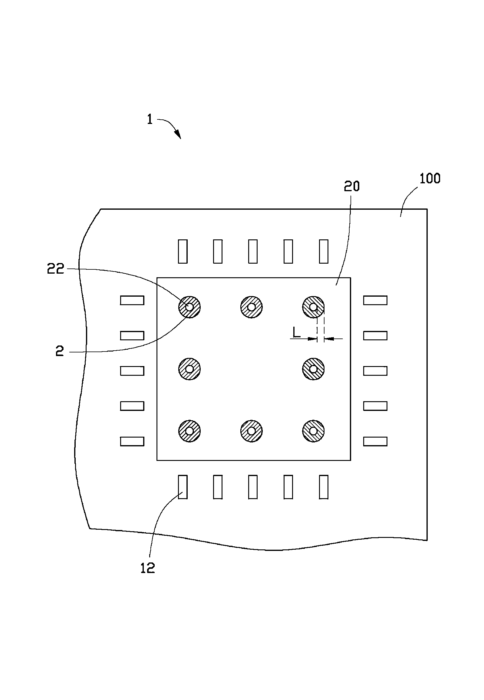
[0012] Please refer to figure 1 , the printed circuit board 1 of the present invention includes a substrate 100 . A mounting area 20 is provided on the substrate 100 for mounting a QFN packaged chip. A plurality of lead pads 12 are arranged around the installation area 20 , and a plurality of heat dissipation vias 22 are arranged on the installation area 20 , and a ring-shaped green oil 2 is arranged around each heat dissipation via 22 . The annular green oil 2 and the corresponding heat dissipation via hole 22 form concentric circles with a radius difference of L. The green oil 2 is solder resist. The rest of the installation area 20 is provided with copper foil. The shape of the green oil 2 is not limited to the ring shape in this embodiment, any shape of green oil can be arranged around the heat dissipation via hole 22 as required, and t...


PUM


Abstract

A printed circuit board (PCB) comprising a base board, the base board defines a thermal pad and a plurality of pin pads for solder an integrated circuit (IC) with a Quad Flat No-lead (QFN) package, wherein a plurality of thermal vias are defined on the thermal pad through the base board, a solder mask is defined around each of the thermal vias.

Description

technical field [0001] The invention relates to a printed circuit board. Background technique [0002] QFN (Quad Flat No-lead) packaged electronic parts are widely used in high-density printing of mobile phones, digital cameras, tablets and other portable small electronic devices due to their small size, light weight, and outstanding electrical and thermal properties. circuit board. [0003] There is a large heat dissipation pad at the center of the bottom of the chip in the QFN package for heat conduction. Usually, the heat dissipation pad is directly soldered to the printed circuit board, and the heat is diffused to the inner heat dissipation layer through the heat dissipation vias on the printed circuit board ( Usually the formation), thereby absorbing excess heat. However, these heat dissipation vias will leak tin during the reflow soldering of the circuit board, which will affect the appearance and even cause a short circuit. Contents of the invention [0004] In v...

Claims


Application Information

Patent Timeline
IPC IPC(8): H05K1/02H05K1/18
CPCH05K1/113H05K2201/095H05K2201/09481H05K2201/0137H05K1/0206H05K2201/06H05K3/3452H05K2201/099H05K2201/09909H05K2201/10727H05K2203/0591
Inventor 赖超荣
Owner HONG FU JIN PRECISION IND (SHENZHEN) CO LTD
Why Eureka
Try Eureka