Semiconductor device and manufacturing method of the same

a technology of semiconductor devices and manufacturing methods, applied in semiconductor devices, semiconductor/solid-state device details, electrical apparatus, etc., can solve the problems of insufficient reliability, prior art, and inability to ensure sufficient reliability for bonding to such interposers

Inactive Publication Date: 2002-09-19
NEC ELECTRONICS CORP
View PDF4 Cites 62 Cited by
  • Summary
  • Abstract
  • Description
  • Claims
  • Application Information

AI Technical Summary

Problems solved by technology

For this reason, sufficient reliability is difficult to ensure.
The underfill technique, however, involves a problem in that a smaller pitch of electrodes 12 (fine pitch), an accompanying smaller size of bumps 13, and a smaller gap between semiconductor chip 11 and interposer 14 result in difficulties in completely filling underfill resin 17 between semiconductor chip 11 and interposer 14 and in checking whether or not any unfilled portion (void) is present after mounting.
In addition, even when any defect occurs after the mounting on an interposer, replacement is readily made individually since the device is not completely fixed to the interposer by an epoxy resin or the like.
The aforementioned prior arts, however, have the following problems.
In mounting on various interposers, however, sufficient reliability cannot be ensured for bonding to such interposers.
In this case, however, the mounting structure is complicated and the number of mounting steps is increased to cause a higher cost.
In addition, as described above, it is difficult to inject the underfill resin between a semiconductor chip and an interposer, and especially for a number of pins of 1000 or more, voids occur frequently and an expensive substrate is readily changed to an unuseful material.
It is difficult, however, to control the position of adhesive sheet 98 such that through-holes 102 are accurately placed between opposing bumps 80 and connection holes 96.
Since such accurate arrangement is more difficult especially as a semiconductor device is miniaturized with a finer pitch of electrodes and smaller bumps, miniaturization of semiconductor devices is obstructed.
While the positioning of the sheet is not required when an anisotropic conductive film is used, a load applied on the bumps at the pressing also tends to cause faulty connection.
Furthermore, in general, an anisotropic conductive film is not so inexpensive.
Thus, according to the method disclosed in Japanese Patent Laid-open Publication No. 11-26642, it is difficult to reliably mount at low cost a semiconductor device with electrodes of high density, for example having 1000-pin electrodes formed in an area of 10 mm.times.10 mm.
Thus, a stud bump method, which is an application of a wire bonding technique cannot be used.
The inability to use the wire bonding technique presents a problem of failing to have the capability of dealing with individual cases and making it difficult to perform flexible manufacturing.
On the other hand, polyimide, BT resin, ceramic and the like as a base material of an interposer are expensive to raise concern about a high proportion of its cost to the product price.
The build-up BT substrate, however, is expensive to raise concern about a high proportion of its cost to the product price.

Method used


Image

  • Semiconductor device and manufacturing method of the same
  • Semiconductor device and manufacturing method of the same
  • Semiconductor device and manufacturing method of the same

Examples


embodiment 1

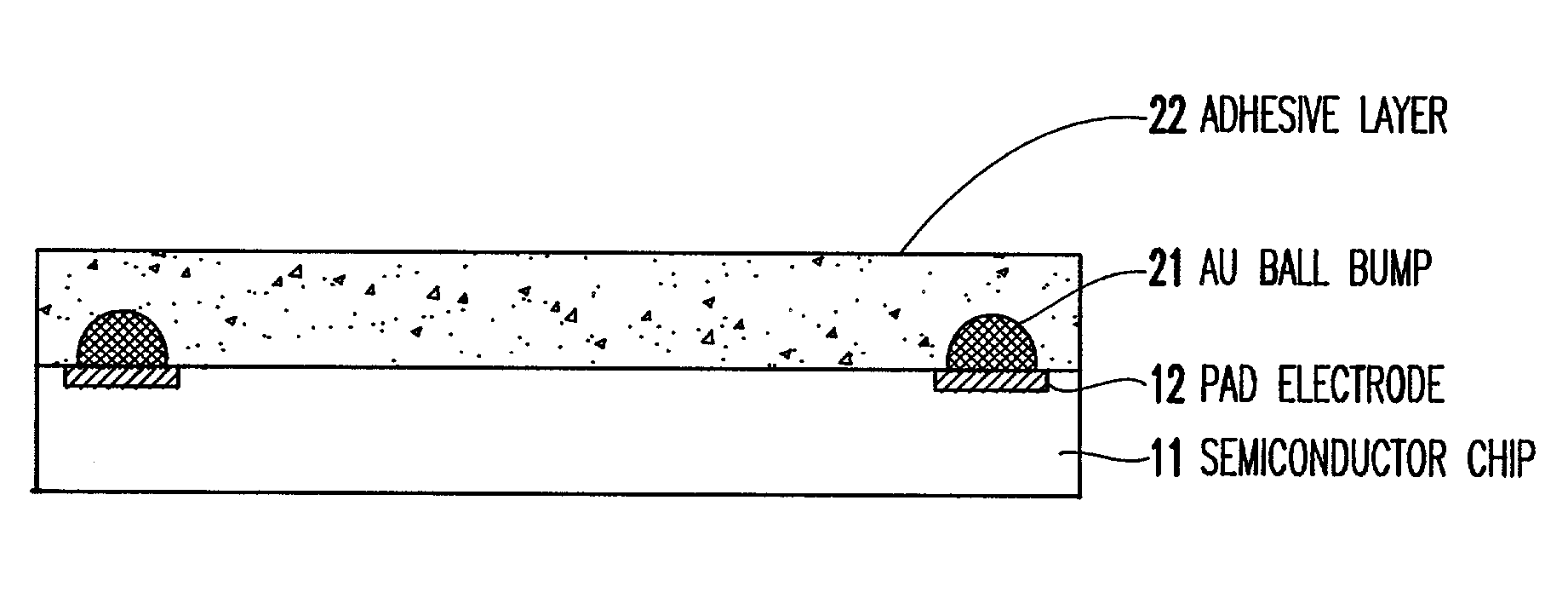
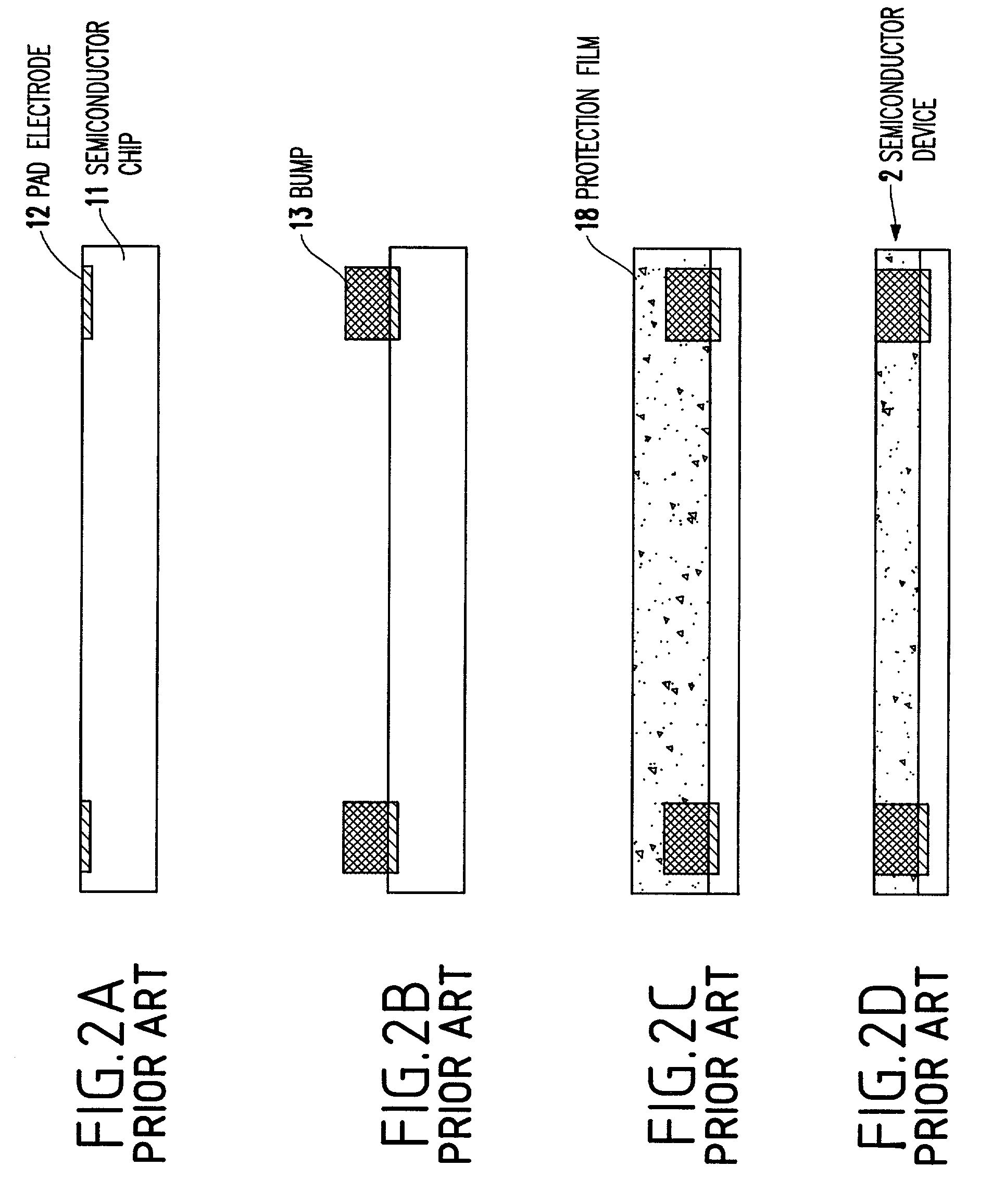
[0183] As shown in FIG. 4(d), semiconductor device 3 (HDP: High Density Package) of Embodiment 1 comprises semiconductor chip 11, Au ball bumps 21 provided on pad electrodes 12 with a stud bump method, and thermoplastic adhesive layer 22 disposed on the surface of semiconductor chip 11 on which pad electrodes 12 are formed such that the tops of Au ball bumps 21 project from the surface of adhesive layer 22.

[0184] While adhesive layer 22 is formed of a thermoplastic adhesive in consideration of replacement of a defective item after adhesion, a thermosetting adhesive may be used instead of the thermoplastic adhesive if such replacement is not required.

[0185] Semiconductor device 3 is manufactured as follows. FIGS. 4(a) to (d) are enlarged views showing one particular semiconductor chip 11 formed in semiconductor wafer 20.

[0186] After a predetermined number of semiconductor chips 11 are manufactured in semiconductor wafer 20, Au ball bumps 21 are provided on pad electrodes 12 of each s...

embodiment 2

[0190] Next, a semiconductor device and a manufacturing method thereof according to Embodiment 2 of the present invention are described with reference to FIG. 5(a). FIG. 5(a) is a cross section showing the semiconductor device of Embodiment 2 of the present invention.

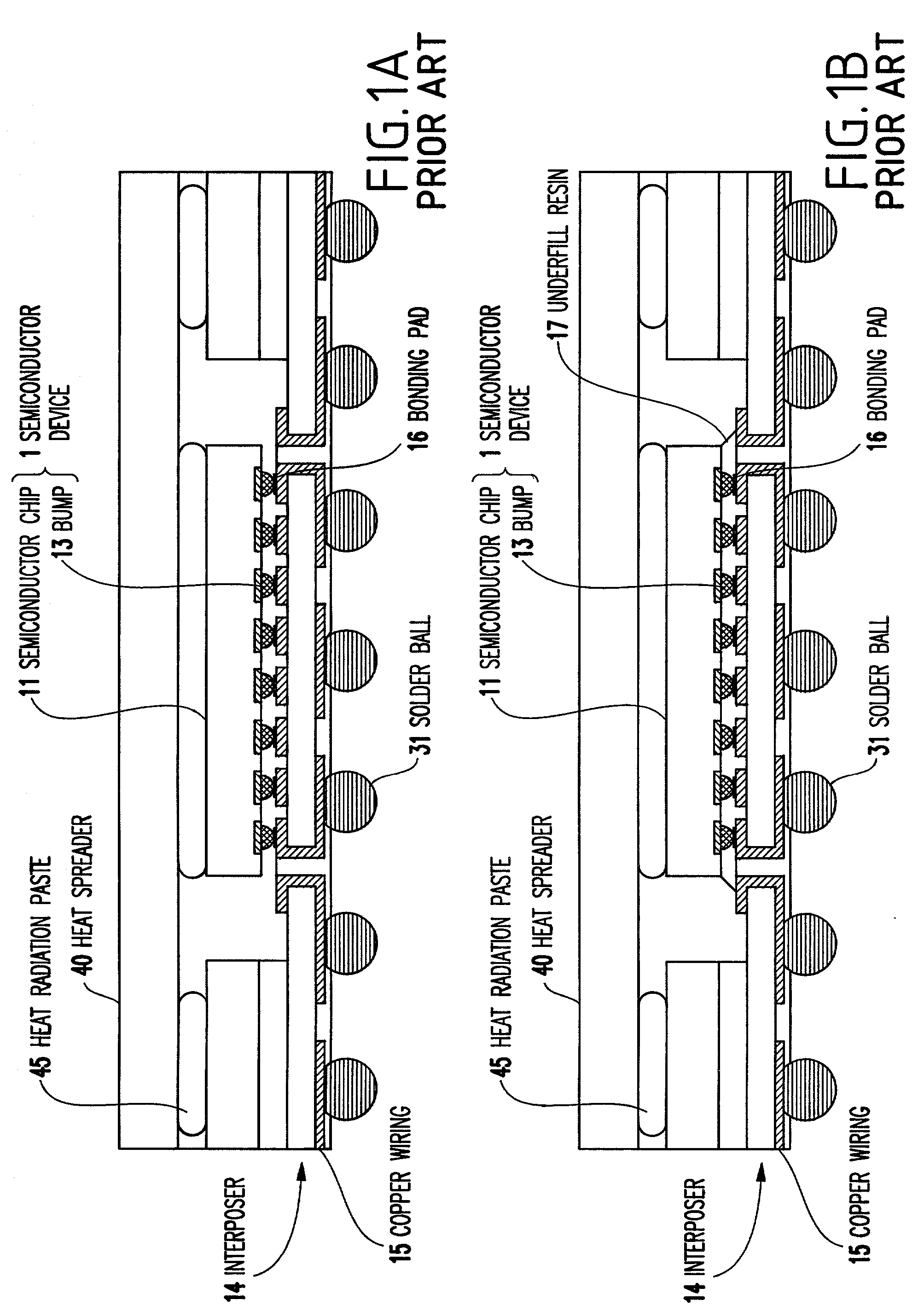
[0191] The semiconductor device shown in FIG. 5(a) is a semiconductor device (BGA type semiconductor package) in which semiconductor device 3 is bonded to wiring tape 23 as an interposer through thermocompression bonding and resin molding is performed. For manufacturing, semiconductor wafer 20 (see FIG. 4) is first cut for division into individual semiconductor devices 3.

[0192] Next, one, or two or more semiconductor devices 3 are mounted on one wiring tape 23, and heating and pressing are performed to establish adhesion to wiring tape 23 with adhesive layer 22 and electrical connection to copper wiring 24 on wiring tape 23 with Au ball bumps 21. Such adhesion and connection may be performed as follows.

[0193] Wiring tap...

embodiment 3

[0203] Next, a semiconductor device and a manufacturing method thereof according to Embodiment 3 of the present invention are described with reference to FIG. 5(b). FIG. 5(b) is a cross section showing the semiconductor device of Embodiment 3 of the present invention.

[0204] The semiconductor device shown in FIG. 5(b) comprises semiconductor chip 11, adhesive layer 22 as a protection resin layer provided on the surface on which pad electrodes 12 are formed, Au ball bums 21 formed on pad electrodes 12 and exposed at the surface of adhesive layer 22, and wiring tape 23 adhered to the surface of adhesive layer 22 through cured flux 28 and serving as an interposer for electrical connection to Au ball bumps 21. The semiconductor device is a semiconductor device (BGA type semiconductor package) manufactured by bonding semiconductor device 3 to wiring tape 23 with thermocompression bonding and performing resin molding.

[0205] For manufacture, semiconductor wafer 20 (see FIG. 4) is first cut ...


PUM


Abstract

Semiconductor device 3 comprises semiconductor chip 11, Au ball bumps 21 formed on pad electrodes 12 with a stud bump method, and thermoplastic adhesive layer 22 provided on the surface of semiconductor chip 11 on which pad electrodes 12 are formed, in which the tops of Au ball bumps 21 project from the surface of adhesive layer 22. Reliable bonding can be realized by forming the bumps for electrical connection and the adhesive resin having an adhesion function on the semiconductor chip. In addition, the present invention provides a method of bonding a copper foil to a semiconductor wafer to form a wiring pattern, a multi chip module in which electrical connection is established by bumps bonded to each other through an adhesive layer, and the like.

Description

[0001] 1. Field of the Invention[0002] The present invention relates to a semiconductor device and a manufacturing method thereof, and more particularly to a high-density type semiconductor device (HDP: High Density Package) of a flip-chip method, a semiconductor device (especially, CSP: Chip Size (Scale) Package) including an HDP mounted on an interposer and a multi chip module (MCM: Multi Chip Module, stacked MCP: Multi Chip Package) including a plurality of HDPs, and a manufacturing method thereof.[0003] 2. Description of the Related Art:[0004] In recent years, research and development work has been conducted on a higher density of mounting in a semiconductor device, and a number of structures and methods have been proposed for package forms or mounting methods. The forms are transitioning from QFPs (Quad Flat Package) which are a typical conventional semiconductor package to BGA (Ball Grid Array) packages of an area array type in response to the needs of an increase in number of...

Claims


Application Information

Patent Timeline
Patent Type & Authority Applications(United States)
IPC IPC(8): H01L23/12H01L21/56H01L21/60H01L21/68H01L23/498H01L25/065
CPCH01L21/563H01L21/6835H01L23/49816H01L25/0657H01L2221/68377H01L2224/1134H01L2224/13144H01L2224/16225H01L2224/73203H01L2224/73204H01L2224/73253H01L2224/83101H01L2224/83102H01L2224/83191H01L2224/92125H01L2225/06513H01L2225/06517H01L2225/06541H01L2225/06555H01L2225/06572H01L2225/06582H01L2225/06586H01L2225/06589H01L2924/01004H01L2924/01005H01L2924/01013H01L2924/01015H01L2924/01025H01L2924/01029H01L2924/01033H01L2924/01039H01L2924/0105H01L2924/01078H01L2924/01079H01L2924/01082H01L2924/15153H01L2924/1517H01L2924/15311H01L2924/16152H01L2924/16195H01L2924/166H01L24/29H01L2224/32225H01L2924/01006H01L2924/01023H01L2924/0132H01L2224/29111H01L2224/13025H01L2224/16145H01L2224/32145H01L2224/32245H01L2924/15321H01L2924/16251H01L2924/15787H01L2224/2919H01L2224/29011H01L2224/73104H01L2224/81191H01L2924/00H01L2924/00014H01L2924/351H01L2224/45144H01L2224/05571H01L2224/05573H01L2224/056H01L2924/181H01L24/05H01L2924/15151H01L2924/00012H01L23/48
Inventor URUSHIMA, MICHITAKA
Owner NEC ELECTRONICS CORP
Why Eureka
Try Eureka