Electrodeposited copper foil with its surface prepared, process for producing the same and use thereof

a technology of electrodeposited copper foil and surface, which is applied in the direction of insulating substrate metal adhesion improvement, manufacturing tools, lapping machines, etc., can solve the problems of surface roughness of the matte side, thin whole copper foil, and mechanical stress on the copper foil, etc., to achieve high peeling strength, eliminate shelf-shape deformation, and overall stability

Inactive Publication Date: 2002-11-05
MITSUI MINING & SMELTING CO LTD
View PDF12 Cites 62 Cited by
  • Summary
  • Abstract
  • Description
  • Claims
  • Application Information

AI Technical Summary

Benefits of technology

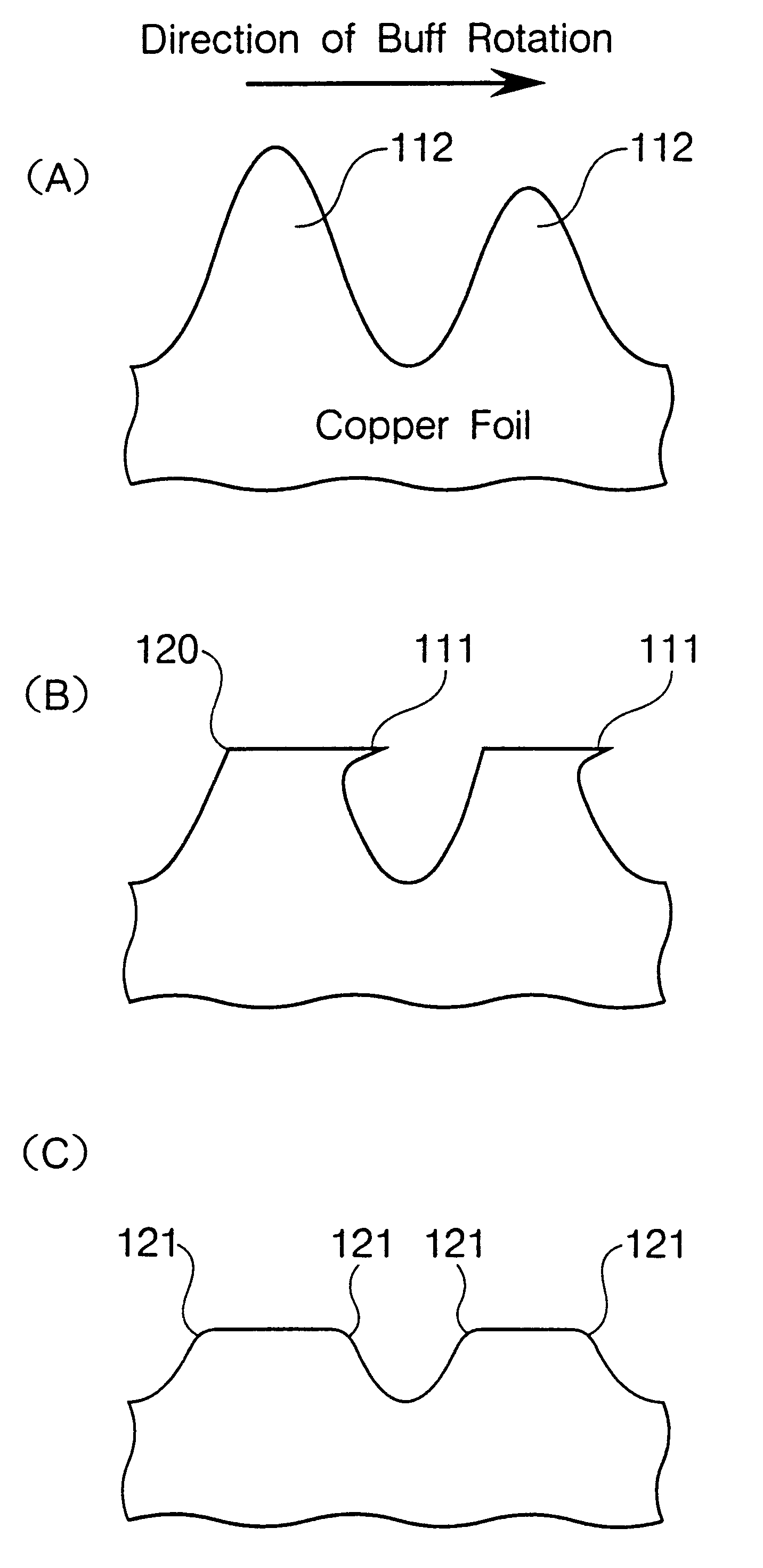
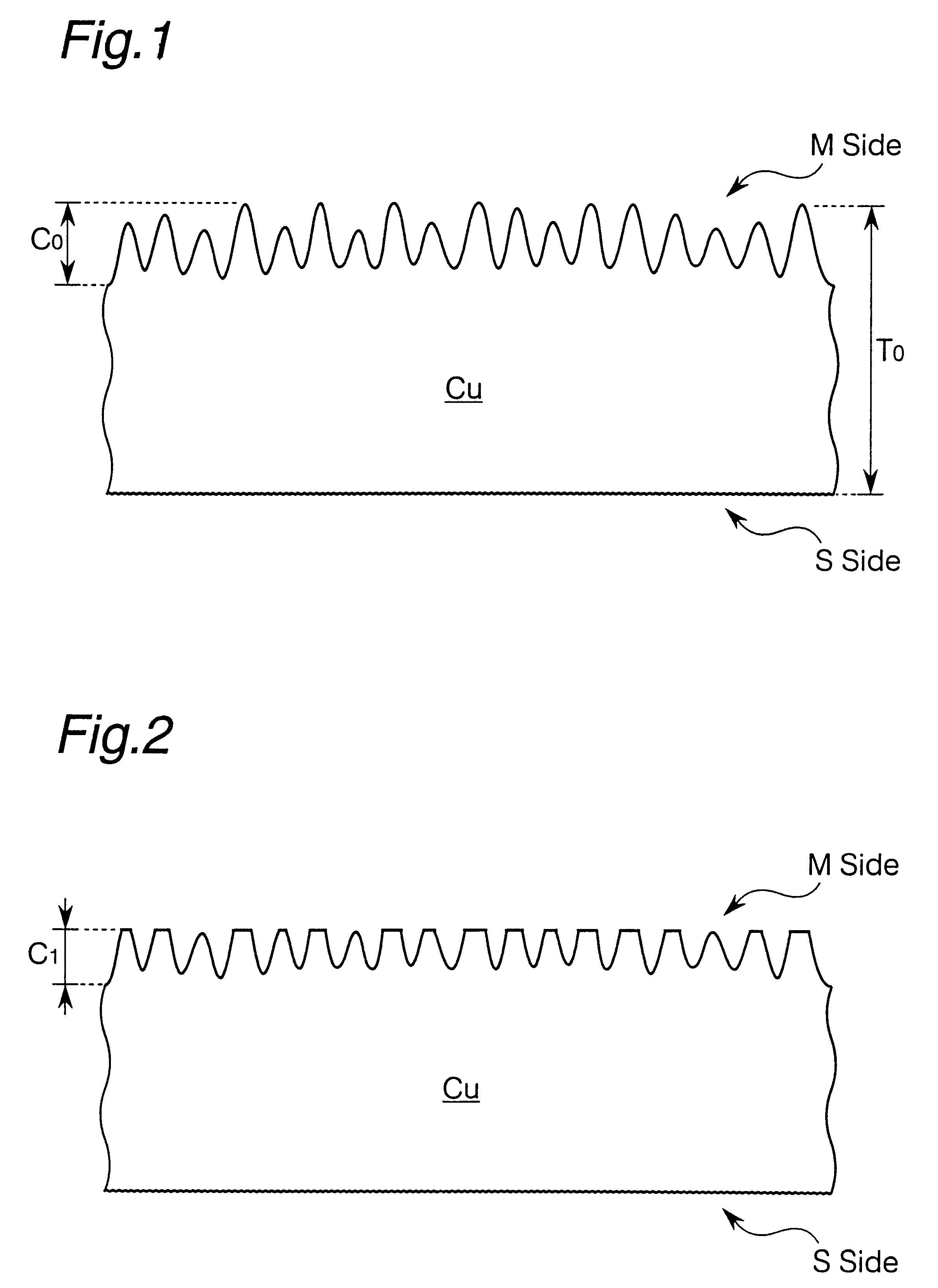
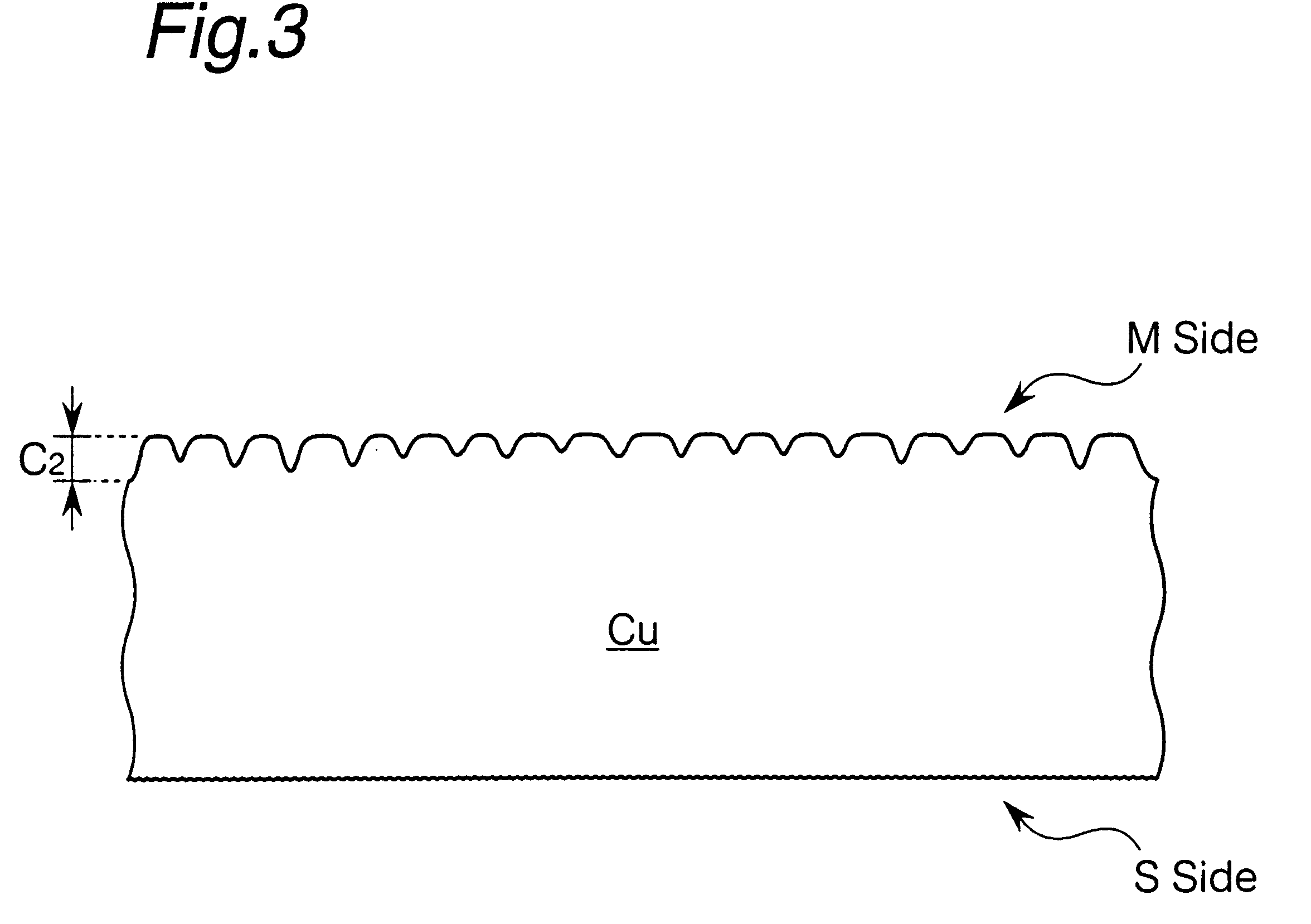
The electrodeposited copper foil with its surface prepared according to the present invention is obtained by sequentially subjecting the matte side to the mechanical polishing and the chemical polishing. The mechanical polishing mainly polishes apex portions of the protrudent parts of the matte side, and the subsequent chemical polishing further uniformly eliminates shelf-shape deformation on the mechanically polished matte side. In the electrodeposited copper foil with its surface prepared according to the present invention, obtained by sequentially subjecting the matte side to the mechanical polishing and the chemical polishing, mechanical polishing traces formed along the mechanical polishing direction and strain layers, generated by the mechanical polishing operation, are eliminated by the chemical polishing to thereby enable forming a strikingly uniform matte side surface. Treating for roughening the thus prepared matte side of the electrodeposited copper foil with its surface prepared enables uniformly forming fine particles of copper on the matte side (electrodeposited copper foil with its surface prepared and treated). The PWB obtained by laminating, for example, an insulating substrate with the thus obtained electrodeposited copper foil with its surface prepared according to the present invention and forming the copper foil into a wiring pattern exhibits a high peel strength between the wiring pattern and the insulating substrate and further ensures an overall stable strength. Moreover, in the process of the present invention, not only are apex portions of the protrudent parts of the matte side mainly mechanically polished but also the polishing irregularity, streaks, strain, etc., resulting from the mechanical polishing, are eliminated by the chemical polishing. Thus, the copper loss by polishing is strikingly slight, and the matte side surface consisting of a continuous curved shape can be obtained.
This roughening treatment of the matte side enables performing uniform nodulating treatment of the prepared matte side. Thus, PWB capable of exhibiting high performance in adhesive strength, bonding reliability, etc. can be obtained.
In the process of the present invention, the matte side of the electrodeposited copper foil is sequentially subjected to the mechanical polishing performed under mild conditions and the chemical polishing, so that the occurrence of streaks and the like on the polished matte side can be suppressed. The streaks are generally attributed to excess polishing, and the electrodeposited copper foil of this part is thinner there than at other parts. Thus, when the electrodeposited copper foil having streaks is employed in the use of an extremely thin copper foil in accordance with the trend toward fine pitch, the mechanical strength of wiring pattern there is reduced with the result that the streak portions are likely to become the cause of failure such as open circuit. The electrodeposited copper foil with its surface prepared, produced by the process of the present invention, is free from such streaks attributed to excess polishing, so that, with respect to wiring boards such as PWB produced with the use of the prepared electrodeposited copper foil, the occurrence of defective items attributed to such an open circuit or the like is strikingly low.
Moreover, when the electrodeposited copper foil with its surface prepared according to the present invention is formed into a wiring pattern through superimposing the same on an insulating substrate by laminating or bonding after resist application and etching, the difference between upper edge width and lower edge width of the formed wiring (especially lead parts) is minute. Thus, a wiring of approximately rectangular cross section can be formed. In the use of the conventional electrodeposited copper foil, the lower edge tends to be larger and wavier than the upper edge in the formed wiring, thereby causing the cross section configuration to be trapezoidal. However, in the use of the electrodeposited copper foil with its surface prepared according to the present invention, the above trend is eliminated, and a wiring of approximately rectangular cross section can be obtained. Furthermore, the lower edge portions of the wiring are etched linearly, and there is substantially no copper residue on the insulating substrate. These characteristics, although important in, for example, inner leads as well, are especially important in output side outer leads electrically connected to liquid crystal elements, and the like. With respect to the output side outer leads electrically connected to liquid crystal elements, a plurality thereof are connected to liquid crystal pixels, and not only is the lead width thereof extremely small but also the pitch is rendered small. Accordingly, the output side outer leads are likely to suffer from insulation failure between neighboring leads. For example, even if the linearity of output side outer leads is slightly deteriorated, there is the danger of insulation failure (short circuit). Further, if the lower edge is slightly wider than the upper edge in the output side outer leads, there is the danger of insulation failure (short circuit) on the surface of the insulating substrate. Still further, even if slight copper residue exists on the insulating substrate, there is the danger of insulation failure (short circuit). In the output side outer lead parts of PWBs (especially TAB tape) connected to liquid crystal elements, etching of the copper foil must be achieved with precision equal to or higher than that for inner leads for mounting electronic components. Especially, with respect to the output side outer leads of the TAB tape for liquid crystal elements, these must be formed on an insulating substrate by etching the electrodeposited copper foil disposed on the insulating substrate by laminating, so that each of the leads is likely to have a trapezoidal cross section as compared with inner leads which extend out into device holes and under which any insulating substrate is not present. Further, due to the presence of the insulating substrate, copper residue is likely to occur. Therefore, it is believed that the achievement of fine pitch is more difficult in the output side outer leads than in the inner leads.
However, the above achievement of fine pitch in the output side outer leads can be enabled by the use of the electrodeposited copper foil with its surface prepared according to the present invention. Specifically, by virtue of the use of the electrodeposited copper foil with its surface prepared according to the present invention, not only do the output side outer leads formed by etching have a rectangular cross section (upper edge width being substantially the same as the lower edge width) but also the linearity of formed leads is high. Further, there is no copper residue on the surface of the insulating substrate. Although the particular reason for the above excellent etching properties of the electrodeposited copper foil with its surface prepared according to the present invention has not yet been elucidated, specific exertion of the above effects of the present invention would be achieved by the mechanical polishing followed by the chemical polishing.
As apparent from the above, the electrodeposited copper foil with its surface prepared, obtained by the process of the present invention, ensures not only high adherence to insulating substrates but also strikingly high yield of device mounting on boards.

Problems solved by technology

In the conventional electrodeposited copper foil of about 35 .mu.m nominal thickness, it has been rare that the surface roughness of the matte side poses a problem.
When use is made of a thin copper foil, the copper foil may be broken by mechanical stress exerted on the copper foil.
Therefore, in this chemical polishing, the whole copper foil tends to become thin.
Accordingly, when the thin electrodeposited copper foil employed in conformity with the recent trend toward fine pitch, for example, the electrodeposited copper foil having a thickness of 35 .mu.m (1 ounce), or 17.5 .mu.m (1 / 2 ounce), or less is chemically polished to such an extent that a desired state of surface is attained, the whole electrodeposited copper foil is thinned to such an extent that the mechanical strength of wiring pattern or lead becomes poor.
Further, this chemical surface polishing poses a problem such that it is difficult to control reaction conditions for chemical polishing so as to have the matte side uniformly treated.
These problems of chemical polishing also occur in the electrolytic polishing involving leaching of copper.
The surface roughness of this non-treated rolled copper foil is too low to ensure satisfactory peel strength (bonding strength).
This poses a problem such that the process becomes laborious.
Further, the use of this rolled copper foil renders it difficult to form a wiring pattern of extremely fine pitch such as one of from 30 .mu.m to less than 60 .mu.m pitch width.
However, the buffing of electrodeposited copper foil at a stretch as described in this publication may cause streaks on the buffed surface.
However, these streak portions are formed by excess polishing of copper, so that, when use is made of thin copper foils, the depth of streak portions is extremely large.
Thus, these are likely to become the cause of defective occurrence, for example, high possibility of open circuit at such portions in a wiring pattern or the like.
Furthermore, in the execution of such buffing, stress is exerted on protrudent parts of the copper foil surface along the direction of buff rotation, so that protrudent parts of the copper foil surface are likely to deform along the direction of buff rotation.
It is difficult to effect uniform roughening treatment on the buffed copper foil having thus deformed protrudent parts.
Nonuniform roughening treatment would invite problems such that the adherence to insulating films, etching uniformity, bonding reliability, etc. are deteriorated.
These problems are likely to occur especially when thin electrodeposited copper foils are mechanically polished.
However, the single employment of the above conventional polishing methods in the polishing of the matte side of the electrodeposited copper foil used to produce a printed wiring board whose pitch is becoming tens of microns or less involves the highly probable danger of causing the formed wiring pattern to be brittle and hence tends to render it difficult to supply printed wiring boards having reliable properties.

Method used


Image

  • Electrodeposited copper foil with its surface prepared, process for producing the same and use thereof
  • Electrodeposited copper foil with its surface prepared, process for producing the same and use thereof
  • Electrodeposited copper foil with its surface prepared, process for producing the same and use thereof

Examples


example 1

An electrodeposited copper foil (VLP foil) of 18 .mu.m gauge thickness having an average surface roughness of shiny side of 1.2 .mu.m and an average surface roughness (Rz.sub.l) of matte side of 3.6 .mu.m was provided. A SEM photo of the matte side of the VLP foil is shown in FIG. 7.

While the VLP foil was being passed through guide rolls, the matte side of the VLP foil was buffed by means of # 1000 buff comprising aluminum oxide as abrasive grains (manufactured by Tsunoda Brush K.K.), arranged so that the direction of buff rotation was counter to the direction of advance of electrodeposited copper foil, under conditions such that the first-stage buff rotating speed, press force in terms of buff motor current value and line speed were 1200 .mu.m, 19 A and 8 m / min, respectively (the first mechanical polishing).

A SEM photo of the matte side having undergone the first mechanical polishing is shown in FIG. 8.

After the first mechanical polishing of the VLP foil, the matte side having unde...


PUM

PropertyMeasurementUnit
surface roughnessaaaaaaaaaa

Abstract

A process for producing an electrodeposited copper foil with its surface prepared, comprising the steps of: subjecting an electrodeposited copper foil having a shiny side and a matte side whose average surface roughness (Rz) is in the range of 2.5 to 10 mum to at least one mechanical polishing so that the average surface roughness (Rz) of the matte side becomes in the range of 1.5 to 3.0 mum; and subjecting the matte side having undergone the mechanical polishing to a selective chemical polishing so that the average surface roughness (Rz) of the matte side becomes in the range of 0.8 to 2.5 mum. The invention further provides an electrodeposited copper foil with its surface prepared, produced by the above process, and still further provides PWBs and a multilayer laminate of PWBs, produced with the use of the above electrodeposited copper foil with its surface prepared. The mechanical polishing followed by chemical polishing of the matte side enables obtaining an electrodeposited copper foil with its surface prepared, the matte side of which exhibits excellent properties, and hence enables obtaining PWBs and a multilayer PWBs which have excellent properties.

Description

The present invention relates generally to an electrodeposited copper foil with its surface prepared wherein a matte side, namely a surface at which copper deposition is completed, is mechanically polished at least once and the thus mechanically polished matte side is subjected to a selective chemical polishing so as to attain preparing thereof, and relates to a process for producing the same and a use of the electrodeposited copper foil with its surface prepared in, for example, a printed wiring board.In recent years, both the size and weight of electronic equipment such as a notebook-sized personal computer are being reduced to increasing extents. Accordingly, IC wiring is also becoming finer.With respect to the wiring pattern formed on a substrate used in such an electronic equipment, the lead width is now as small as ten-odd microns (.mu.m). In accordance therewith, the metal foil constituting the wiring pattern is becoming thinner. Specifically, while the designated thickness o...

Claims


Application Information

Patent Timeline
Patent Type & Authority Patents(United States)
IPC IPC(8): C25D1/04C25D5/48H05K3/38B24B37/00C23F1/18C25D7/06H05K1/09
CPCC25D1/04C25D5/48H05K3/382Y10T428/12438Y10T428/12993Y10T428/1291Y10T428/12569Y10T428/12472Y10T428/12431C25D7/06
Inventor MITSUHASHI, MASAKAZUMASHIKO, YASUAKIKURABE, HITOSHI
Owner MITSUI MINING & SMELTING CO LTD
Why Eureka
Try Eureka