PCB testing device

A technology for testing devices and PCB boards, applied in the direction of measuring devices, measuring electricity, and measuring electrical variables, etc., can solve the problems of not being able to see the real problems of PCB boards, low detection efficiency, and high labor intensity, so as to improve work efficiency and test Accuracy, high degree of automation, and the effect of reducing labor intensity

Active Publication Date: 2014-11-12
KUSN MAIZHI FIXTURE TECH
View PDF8 Cites 9 Cited by
  • Summary
  • Abstract
  • Description
  • Claims
  • Application Information

AI Technical Summary

Problems solved by technology

[0003] The traditional PCB board debugging method mainly uses human eyes to inspect the missing soldering of the main components of the PCB board and the open and short circuits of the circuit. However, this method not only has low detection efficiency, but also has high labor intensity, error-prone, and low accuracy. And it is impossible to see the real problem in the PCB board

Method used


Image

  • PCB testing device
  • PCB testing device
  • PCB testing device

Examples


Embodiment 1

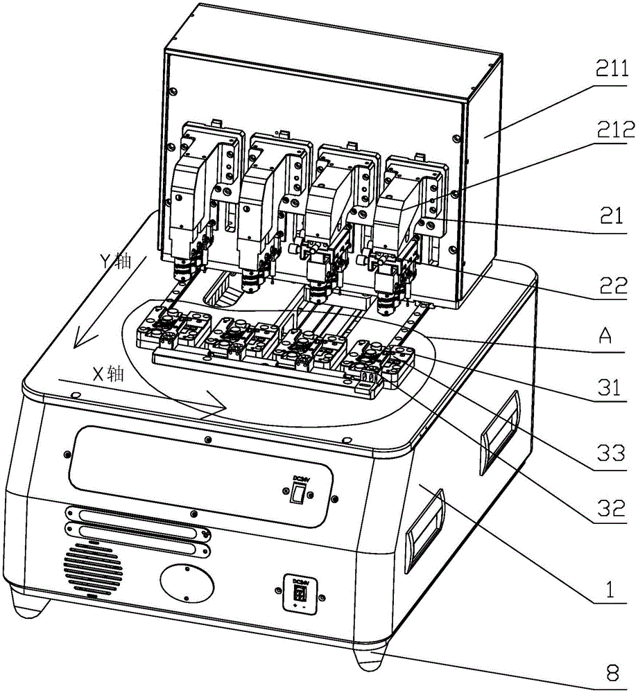
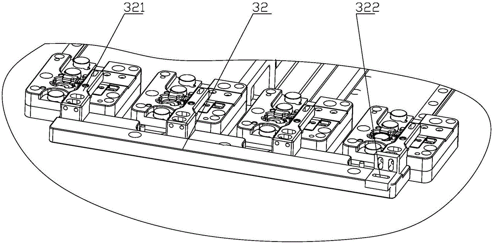
[0034] The present embodiment provides a kind of test device of PCB board, the structure of the test device of this PCB board is as follows Figure 1-Figure 8 As shown, it includes an electric control box 1, an upper mold assembly arranged above the electric control box 1 and a lower mold assembly arranged on the upper panel of the electric control box.

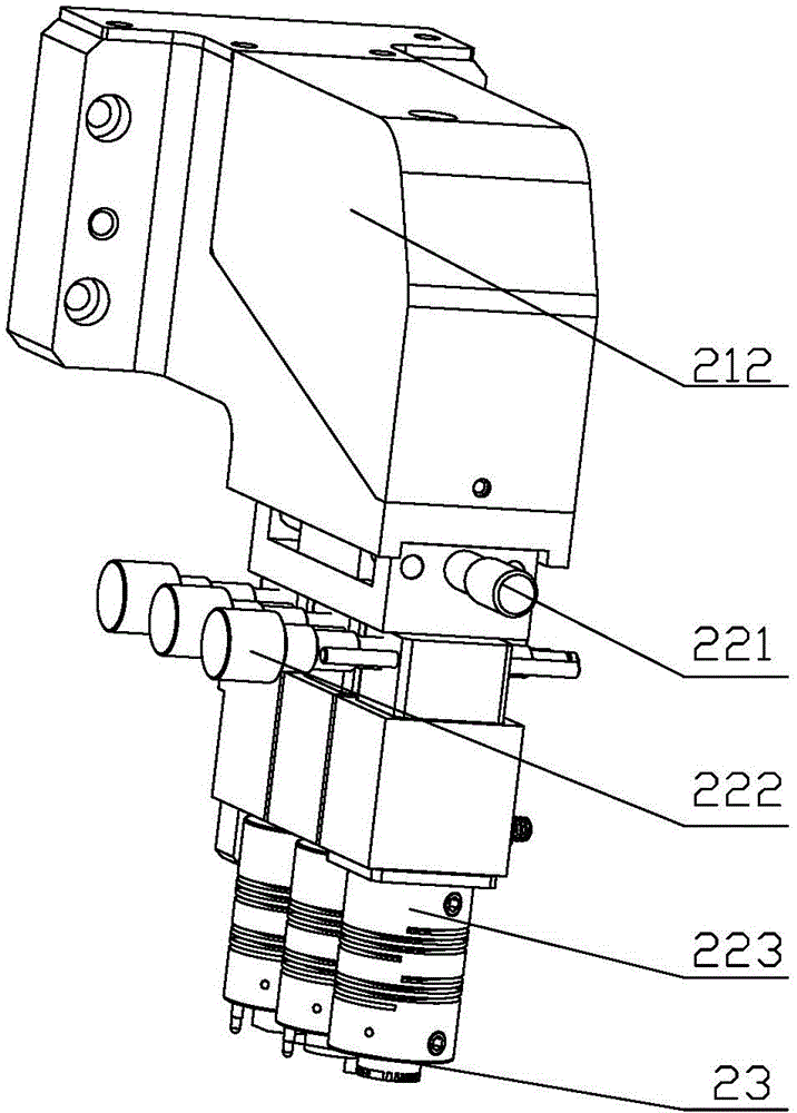
[0035] The upper mold assembly includes four sets of lifting mechanisms 21 , four sets of XY axis moving mechanisms 22 and four sets of probes 23 corresponding to the lifting mechanisms 21 and XY axis moving mechanisms 22 , and each set of probes 23 includes three probes 23 . The lifting mechanism 21 is used to drive the probe 23 to move up and down. It includes a fixed seat 211 and a lifting cantilever 212 slidingly connected with the fixed seat 211. The fixed seat 211 is provided with a linear guide rail. The linear guide rail is arranged perpendicular to the upper panel of the electric control box. The cantilever 212 can s...


PUM


Abstract

The invention discloses a PCB testing device and belongs to the technical field of testing devices. The problems that a traditional PCB debugging method is low in detection efficiency, large in labor intensity, low in precision and the like are solved. The PCB testing device comprises an upper mold assembly and a lower mold assembly, wherein the upper mold assembly is arranged above an electric control box, and the lower mold assembly is arranged on an upper panel of the electric control box. Under the effect of a lifting mechanism and an XY axis moving mechanism of the upper mold assembly, a probe on the upper mold assembly is made to penetrate through a probe hole in a probe board of the lower mold assembly, so that the probe makes contact with a product to be tested on a product carrier board for testing the situations such as lack of weld and open-short circuits of main elements of the PCB. The PCB testing device is easy to operate and high in automation degree, simplifies manual operation, reduces labor intensity and improves working efficiency and testing accuracy.

Description

technical field [0001] The invention relates to a test device, in particular to a test device for a PCB board. Background technique [0002] With the advancement of science and technology, the development of the electronic industry is advancing by leaps and bounds, the electronic system is becoming more and more complex, and the reliability and maintainability requirements of the electronic system are also getting higher and higher. As an important part of the development and production of electronic systems, the quality of PCB boards directly affects the quality of the entire equipment, and the long production cycle will affect the debugging progress and delivery time of the whole machine. Therefore, PCB board debugging is an important link related to the quality and production cycle of the electronic system. [0003] The traditional PCB board debugging method mainly uses human eyes to inspect the missing soldering of the main components of the PCB board and the open and s...

Claims


Application Information

Patent Timeline
Patent Type & Authority Applications(China)
IPC IPC(8): G01R31/02
Inventor 周卫华刘灿狄静王盛胡志刚
Owner KUSN MAIZHI FIXTURE TECH
Why Eureka
Try Eureka