Capacitive touch screen and preparation method thereof
A capacitive touch screen and touch area technology, which is applied in the input/output process of electrical digital data processing, instruments, and data processing, etc. Yield and production capacity and other issues, to achieve the effect of electrode pattern and trace optimization, high light transmittance, and reliable structure
- Summary
- Abstract
- Description
- Claims
- Application Information
AI Technical Summary
Problems solved by technology
Method used
Image
Examples
Embodiment 1
[0039] A method for preparing a capacitive touch screen with a compound touch electrode structure according to the present invention comprises the following steps:
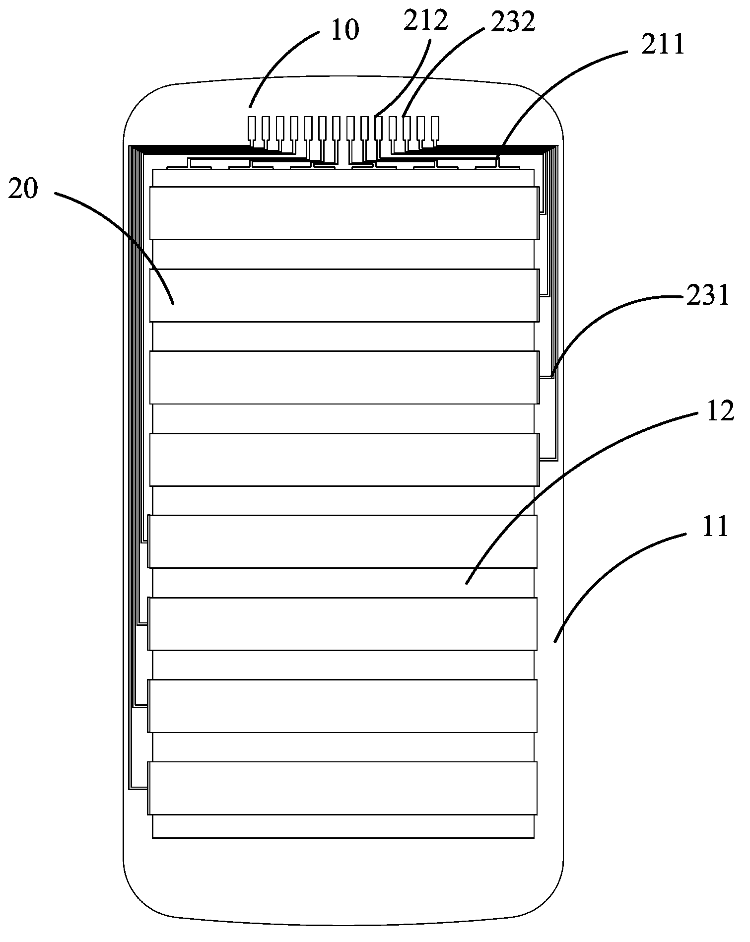
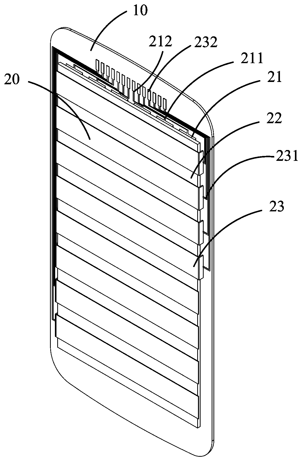
[0040] 1. A non-window ink area 11 is formed around the single substrate, and the middle area surrounded by the non-window ink area 11 is the window touch area 12, and the thickness of the ink is 0.005 mm to 0.1 mm;
[0041] The monolithic substrate of the present invention can be made of glass with a thickness of 0.4 mm to 1.2 mm, preferably 0.7 mm ± 0.1 mm and 1.1 mm ± 0.1 mm. In a specific embodiment, the single substrate is a single panel glass with a thickness of 0.7 mm, which is chemically hardened to make a hardened panel glass with a surface hardness greater than 6H. After cleaning, the surface is screen-printed with ink to form a non-window ink area with surrounding ink and a central transparent window touch area, using high-temperature ink, screen printing twice, with a thickness of 0.02mm; the ink is an...
Embodiment 2
[0055] The difference from Embodiment 1 is that the method further includes a silver paste or metal plating on the first lead-out layer 211 area of the non-window ink area 11 to form electrodes of the first lead-out layer 211 . The fabrication of the electrodes of the first lead-out line layer 211 can be completed before the formation of the first transparent conductive film, or can be completed after the formation of the first transparent conductive film. In a specific embodiment, the non-window ink area 11 uses mask sputtering metal; preferably, the sputtering metal is a combination of copper and molybdenum, the thickness of the copper film is 0.015um, and the thickness of the molybdenum film is 0.005um. It is also possible to sputter a metal molybdenum-aluminum-molybdenum composite film layer on the non-window ink area 11 after masking the window touch area 12 with a film thickness of 0.03 um.
Embodiment 3
[0057] The difference from Embodiment 1 is that the method further includes a process of silk-screen printing silver paste or metal plating on the area of the second lead-out line layer 231 in the non-window ink area 11 to form the electrodes of the second lead-out line layer 231 . The fabrication of the electrodes of the second lead-out line layer 231 can be completed before the formation of the second transparent conductive film, or can be completed after the formation of the second transparent conductive film. In a specific embodiment, the second lead-out line layer 231 is formed on the surface of the non-window ink area 11 covered with SiO2 using a silk screen printing silver paste routing process;
PUM
| Property | Measurement | Unit |
|---|---|---|
| Thickness | aaaaa | aaaaa |
| Thickness | aaaaa | aaaaa |
| Thickness | aaaaa | aaaaa |
Abstract
Description
Claims
Application Information


